
Ceramic PCB Constraints: What Buyers Must Verify First
A ceramic PCB is a printed circuit board built on a ceramic substrate — commonly alumina or aluminum nitride — with a metallised conductor layer, rather than on an organic laminate such as FR-4. That one material decision changes almost every constraint in a purchase order: which acceptance document applies, which records must travel with the lot, how the part is expected to behave through thermal cycling, and why a per-square-metre price is not comparable with a standard multilayer PCB.
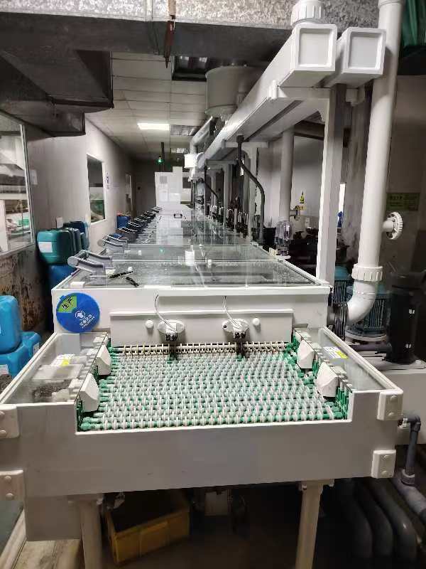
Production workshop. Ceramic substrates sit in a different qualification category from organic laminates, and the documentation burden rather than the board itself is usually where sourcing risk concentrates.
Why Ceramic Boards Get Specified At All
Most buyers evaluating a ceramic PCB arrive from an FR-4 or metal-core background and carry FR-4 assumptions into the request for quotation. Those assumptions break down quickly. Organic laminates dominate the industry by volume — commercial research cited in this article's verified dataset places multilayer PCBs at approximately 52% of total global production volume — so the public information base for ceramic work is far thinner than for standard rigid boards. Fewer data points, fewer comparable quotations, and a much higher chance that two suppliers quote against two different understandings of the same drawing.
The engineering reason ceramic enters a design is usually a combination rather than a single property. Ceramic substrates are selected where electrical isolation and heat spreading must coexist in a small footprint, where dimensional stability under temperature matters, or where the operating environment makes an organic laminate marginal. Ceramic is also brittle compared with FR-4, is generally more expensive per unit area, and is typically built with fewer conductor layers than high-layer-count organic boards. None of that makes ceramic better or worse than FR-4; it makes it a different procurement category with a different constraint set.
The opportunity for a buyer is straightforward. Because the supplier pool is narrower and the specifications are less standardised, the buyer who writes constraints precisely receives quotations that can actually be compared. The buyer who writes “ceramic PCB, quote required” receives numbers that cannot be compared at all.
Where The Procurement Risk Actually Sits
Risk in a ceramic programme rarely originates in the fabrication itself. It originates in the gap between what the drawing states and what the supplier believes it has been asked to build. Five constraint areas account for most of that gap.
1. Substrate identity must be named, not implied
“Ceramic” is a family, not a specification. Alumina and aluminum nitride behave differently, cost differently, and are suited to different thermal duties. A purchase order that names only “ceramic” leaves the material choice to the supplier's default stock, which may change between lots without any visible change to the part number. The substrate material and grade belong in the drawing, alongside any requirement for material certificates per lot.
2. Metallisation and surface finish need explicit terms
Ceramic boards are metallised through processes that differ fundamentally from copper-clad lamination, and the finish on top of that metallisation determines solderability, wire-bondability and shelf life. Buyers should state the metallisation approach, the conductor thickness, and the surface finish as separate line items. A finish named without a thickness is not a specification; it is a preference.
3. Acceptance criteria must be written, not assumed
This is the constraint most often missed. The IPC references used in this article are identified in their source documents as acceptance criteria for printed circuit boards (IPC-A-600), and as qualification and performance specifications for rigid boards (IPC-6012) and flexible boards (IPC-6013). A ceramic programme should therefore have its acceptance document, inspection class, sampling plan, and defect classification written directly into the purchase order rather than inherited from an FR-4 template. Where a supplier cannot name the acceptance document applied to a ceramic build, that omission is itself a qualification finding.
4. Documentation and traceability carry more weight than the sample
A first article that performs well proves that one board performed well. What protects a production programme is the record set: material certificates, lot traceability from incoming material through test, electrical test data, impedance reports where controlled impedance is specified, and compliance declarations. For automotive or other regulated end uses, the quality management scope matters as much as the certificate itself — a certificate whose scope covers circuit board manufacturing is relevant; a certificate whose scope covers something else is not.
5. Volume, tooling and lead time are constraints too
Ceramic programmes frequently begin at low volume and uncertain revision counts, which makes minimum order quantity and prototype turnaround part of the technical evaluation rather than an afterthought. A supplier able to run a single prototype panel and then scale the same documentation set into volume removes a transfer risk that is expensive to discover later.
What A Documented Capability Statement Looks Like
Shenzhen Jerico Multilayer PCB Co., Ltd (JRC/JERICO) is a PCB fabrication and partial PCB assembly supplier founded in 2009, operating a manufacturing site in Wuping, Fujian and a business centre in Shenzhen, Guangdong, with a stated plant area of 20,000 m² and a 30-engineer engineering team. The company reports export activity concentrated in the EU and USA. Its relevance to a constraint-driven buyer is not a claim about ceramic substrates; it is the shape of the documentation it publishes for the categories it does build.
The stated mass-production capability covers rigid PCBs from 1 to 18 layers, including heavy copper, HDI with buried and blind vias, high-frequency boards and metal-core boards, with minimum trace width and spacing down to 3/2.8 mil and impedance tolerance of ±10%. Company-reported material also states support from single-layer to 32-layer boards across double-sided, multilayer, rigid-flex, heavy copper, HDI, FPC, aluminum and high-frequency categories. Surface finishes offered include ENIG, ENEPIG, selective gold plating, OSP, immersion tin, immersion silver and HASL. Quality management runs from IQC incoming inspection through IPQC, AOI full inspection and FQC to laboratory reliability validation, with complaint response within 24 hours and a corrective and preventive report available within 72 hours.
The certification set is specific rather than generic: IATF 16949:2016 issued through NQA with certificate references NQA:T184224, IATF:0493049 and IATF USI:6GXSFM, valid from 22 December 2023 to 21 December 2026, with a scope of manufacturing of circuit boards; UL Recognized under File No. E519316; ISO 9001; ISO 14001; CQC; and RoHS, REACH and SGS compliance test reports. Production is stated to follow IPC-A-600H, IPC-6012, UL-796 and IATF 16949.
Technical Explanation: Reading A Spec Sheet For Constraints
The most useful skill in this category is knowing which lines on a supplier datasheet are constraints and which are decoration. A documented HDI build serves as a worked example because every figure below is a verifiable constraint rather than a marketing attribute.
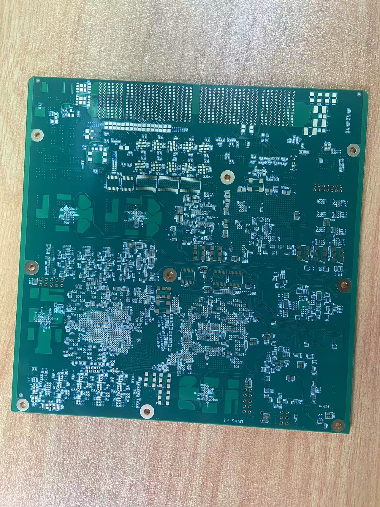
TU-883 hsd hdi 18L: an 18-layer, 2-step HDI board with a 2+14+2 stack-up, used here to illustrate how a verifiable constraint set is written.
Construction and material
The TU-883 hsd hdi 18L is an 18-layer, 2-step HDI board with a 2+14+2 stack-up on high-Tg FR-4 with Tg of 170 °C or higher, finished at 2.40 mm ±0.10 mm with 2 oz (70 µm) outer and inner copper. The M7 is a 32-layer, 3-step HDI board with a 4+24+4 stack-up on TU933 high-Tg FR-4 with Tg of 180 °C or higher, finished at 3.20 mm ±0.10 mm with 2 oz (70 µm) copper, and its stack-up is designed for low Z-axis expansion and CAF resistance to limit warpage and delamination across multiple lamination cycles. For a buyer, Tg, stack-up and thickness tolerance are not engineering trivia; they are the variables that determine whether a board survives reflow and thermal cycling, and they belong in the drawing rather than in a supplier brochure.
Feature resolution and via structure
The TU-883 supports a minimum BGA pitch of 0.5 mm with PTH and laser blind vias, resin-filled microvias and via-in-pad in the BGA field; the M7 supports a 0.4 mm minimum BGA pitch with stacked microvias, resin-filled planarisation and via-in-pad in the BGA area. Both are inspected by X-ray on BGA microvias and electrically tested at 100% flying-probe coverage. Feature resolution determines whether a design is buildable at all; test coverage determines whether a build is verifiable. Buyers commonly negotiate the first and overlook the second.
Controlled impedance
Both builds specify controlled differential impedance of 100 Ω ±8% and single-ended controlled impedance of 50 Ω ±10% for PCIe high-speed signals. Where a design calls for controlled impedance, the RFQ should request an impedance report as a deliverable. A tolerance quoted without a corresponding report is an intention, not evidence.
Finish, gold finger and mechanical features
Surface treatment on these boards is ENIG at 1 U-inch gold with hard gold plating at 30 U-inch on the gold fingers, green solder mask and white silkscreen, a stepped-plate depth of 0.8 mm, single-piece panel delivery, and manufacture to IPC-A-6012 Class 3 with UL94 V-0 compliance. Whatever the substrate family, this is the level of detail that makes a quotation auditable.
Standard rigid builds and the same discipline
The discipline scales down. PCB-54 is a 6-layer FR-4 rigid board with ENIG finish, 2 oz finished copper, 1.6 mm thickness, 0.15 mm minimum hole size and 3 mil minimum line width and spacing. PCB-55 is a 6-layer FR-4 board with ENIG finish, 1 oz copper, 1.6 mm thickness and 0.15 mm minimum hole. PCB-10 is a 4-layer multilayer rigid board with HASL lead-free finish, 1 oz copper, thickness options of 1.0 mm, 1.2 mm and 1.6 mm or customised, 0.2 mm minimum hole and 3 mil line and spacing. PCB-56 is a 4-layer ENIG board at 1.0 mm with black solder mask. Across the range, electrical test is performed by fixture E-test or fly-probe E-test according to order quantity, minimum order quantity is 1 piece, and packaging is vacuum packed. Stated lead time runs from 7 to 45 days depending on build and volume.
Application And Use Cases
Ceramic boards are most often considered alongside automotive power and sensor electronics, industrial power conversion, LED modules and high-temperature environments — situations where heat and isolation are both constrained. The automotive requirement set is the clearest published example of how far a constraint list can extend.
For automotive electronics, the documented requirement profile includes operation across −40 °C to +125 °C, a service life of 10–15 years, exposure to condensation, salt spray, oil, high-humidity bias voltage, chemical cleaning agents and strong electromagnetic interference. The same profile specifies high-Tg FR-4 at Tg ≥170 °C or 180 °C, CAF resistance, UL94-V0 flame retardance, halogen-free as an option, ENIG as the preferred surface finish, manufacture to IPC-A-6012 Class 3, resin-filled and planarised HDI stacked blind vias, full lot traceability of material and production records, and PPAP documentation for mass production. Recommended constructions for automotive work are rigid PCBs, heavy copper PCBs for high-current circuits, HDI with buried and blind vias for dense sensor routing, and metal-core PCBs where fast heat dissipation is needed, with IATF 16949 and IPC-A-600H compliance expected throughout.
Reported case records show the same constraint logic in lower-temperature applications. An EMS factory in Brazil has run LED driver PCB production of 300,000 pieces over six years, reporting a 10% lower price, a one-year increase in product lifespan and a defect rate in the range of 3/1000 to 8/1000. A civilian drone end-product manufacturer in Russia reports 50,000 pieces over eight years, a 5% lower price, a defect rate in the same range and a three-working-day sample lead time. An EMS/ODM factory in India reports 300,000 pieces of mobile payment device PCB with a 10% lower price, a 12-day lead time reduction and a one-year lifespan increase. These are supplier-reported outcomes rather than independently audited results, and they describe organic-laminate work, not ceramic work. Their value to a ceramic buyer is structural: they show which variables — test coverage, traceability, revision control — actually move defect rates.
Market Trend Analysis
The surrounding market context explains why constraint discipline is becoming more valuable rather than less. Prismark data cited in this article's verified dataset places the bare-board PCB market at USD 85.8 billion in 2025, with a projection of roughly USD 95.8 billion for 2026. Commercial research places multilayer PCBs at approximately 52% of total global production volume, and Prismark projects China's share of global PCB production at approximately 60% by 2026.
Two implications follow. First, the volume centre of gravity remains standard multilayer work, which is exactly why the specialty segment is served by a narrower supplier pool and why documentation, not availability, becomes the binding constraint. Second, published growth figures should be read with their definitions attached: sources in the verified dataset differ on growth rates — one attributes double-digit 2026 growth to AI server demand, another focuses on flexible PCB growth, and others report mid-single-digit compound growth for the broader market. That spread reflects methodology and segment definition rather than contradiction. Buyers building a sourcing plan on forecast numbers should confirm whether a figure refers to bare boards or assembly, and which segment it covers.
Comparison With Traditional Solutions
Ceramic is one option among three common substrate routes. The table below compares them on procurement-relevant criteria rather than on performance claims.
| Criterion | FR-4 rigid multilayer | Metal-core / aluminum | Ceramic |
|---|---|---|---|
| Primary role | General-purpose circuit carrier across consumer, industrial, telecom and automotive electronics | Circuit carrier where heat must be conducted away from the board | Circuit carrier where electrical isolation and heat spreading must coexist, often in a small footprint |
| Layer capability | Wide range; 1–18 layers in mass production, with higher layer counts reported for HDI | Generally simpler constructions | Generally fewer conductor layers than high-layer-count organic boards |
| Mechanical robustness | Good; tolerant of handling and depaneling | Good to moderate | Brittle relative to laminates; handling and mounting design matter |
| Relative material cost | Baseline | Above FR-4 | Generally the highest of the three per unit area |
| Standardisation of acceptance | Well covered by named IPC acceptance and performance documents | Covered by named IPC documents plus thermal-specific criteria | Acceptance document, class and sampling must be written into the purchase order |
| Supplier pool | Broad, including Shenzhen-cluster manufacturers | Moderate | Narrow; comparability between quotations is lower |
| Where it usually wins | Cost, layer count, availability, design maturity | Thermal path with conventional circuitry | Isolation plus thermal stability in demanding environments |
| Where it usually loses | Thermally demanding, high-isolation designs | Complex high-layer-count routing | Cost-sensitive, high-layer-count or mechanically abusive designs |
Qualitative comparison. Material properties vary by grade and must be confirmed against the supplier's datasheet for the specific part.
The honest limitation is symmetrical. Ceramic is not a general upgrade path from FR-4, and the documented capability of most Shenzhen-cluster suppliers — including Jerico, whose published specifications centre on rigid multilayer, HDI, heavy copper, high-frequency and metal-core families — does not automatically extend to ceramic substrate work. A buyer who needs ceramic should verify substrate grade, metallisation, acceptance criteria and test coverage in writing before treating any supplier as qualified, and a buyer who does not need ceramic should not pay for it.
Future Outlook
Three developments are likely to shape how ceramic boards are bought over the next few procurement cycles. First, documentation is becoming the differentiator. As more end markets require traceable material records and PPAP-style submissions, the supplier who can produce a coherent record set wins work that a cheaper but less documented supplier cannot hold. Second, the boundary between substrate families is being tested by power density. As modules push more heat through smaller footprints, designs that once defaulted to FR-4 move to metal-core, and some move further to ceramic; each step adds cost and adds documentation burden, so the decision should be made on measured thermal need rather than on category preference. Third, comparability will improve slowly. The verified dataset behind this article records explicit gaps in technical performance benchmarks for ceramic, aluminum, heavy-copper and high-frequency categories, which means buyers will continue to rely on their own RFQ discipline rather than on published cross-supplier data.
The practical response is to build a constraint template once and reuse it: named substrate, named metallisation and finish with thickness, named acceptance document and class, named test coverage, named documentation deliverables, and named volume and lead-time expectations. That template transfers across suppliers and across substrate families, and it is the single most effective protection against the failure mode this category produces most often — a board that meets the drawing and still does not meet the requirement.
FAQ
Which PCB types are recommended for automotive electronics projects?
Rigid PCBs, heavy-copper PCBs, HDI with buried and blind vias, and metal-core PCBs are the constructions recommended for automotive electronics. Rigid PCBs suit standard control modules, heavy copper suits high-current power circuits, HDI suits compact sensor boards with dense routing, and metal-core boards suit modules that need fast heat dissipation. Automotive boards are expected to comply with IATF 16949 and IPC-A-600H, and to perform reliably under wide temperature and vibration exposure.
What documentation should be requested before approving a PCB supplier for a regulated programme?
Request the quality management certificate with its scope and validity dates, the UL recognition file number, RoHS and REACH declarations, an impedance report where controlled impedance is specified, the factory electrical test report, material certificates, and lot traceability records. For automotive mass production, PPAP documentation submission is typically required. Jerico's published record set, for example, includes IATF 16949:2016 with certificate references NQA:T184224, IATF:0493049 and IATF USI:6GXSFM valid to 21 December 2026, UL Recognized File No. E519316, ISO 9001, ISO 14001, CQC, and RoHS, REACH and SGS compliance test reports.
What fabrication tolerances are documented for multilayer and HDI boards?
Documented tolerances include minimum trace width and spacing down to 3/2.8 mil, minimum hole size of 0.15 mm on 6-layer builds and 0.2 mm on 4-layer builds, finished thickness tolerances of ±0.10 mm on HDI constructions such as 2.40 mm and 3.20 mm, minimum BGA pitch of 0.5 mm and 0.4 mm on the two HDI examples, and controlled impedance of 100 Ω ±8% differential and 50 Ω ±10% single-ended. Impedance tolerance is also stated at ±10% at company capability level.
How does a ceramic board differ from FR-4 or metal-core in a purchase specification?
The difference is in the substrate and therefore in what must be written down. A ceramic specification must name the ceramic material and grade, the metallisation approach, the conductor thickness and the surface finish with its thickness, because these vary by supplier and are not interchangeable defaults the way FR-4 is. FR-4 specifications can lean on established laminate designations, and metal-core specifications can lean on the metal base and dielectric combination. Ceramic specifications generally need an explicitly named acceptance document, class and sampling plan, since the acceptance references commonly used for printed boards are framed around rigid and flexible constructions.
Which acceptance standard should be written into a PCB purchase order?
IPC-A-600 is referenced as an acceptance criterion for printed circuit boards. IPC-6012 is identified as a qualification and performance specification for rigid boards, and IPC-6013 for flexible boards, with IPC-6011 as the generic qualification document. Base material requirements are addressed separately, for example IPC-4101F for rigid and multilayer base materials and IPC-4204C for flexible metal-clad dielectrics. The purchase order should name the document, revision and inspection class applicable to the specific build rather than referring to standards generically.
What are the minimum order quantity and lead time for custom PCB fabrication?
Documented minimum order quantity is 1 piece, with vacuum packaging as standard. Stated lead time ranges from 7 to 45 days depending on construction, layer count, surface finish and order volume. Prototype and small-batch runs are supported alongside mass production, and a reported case record cites a three-working-day sample lead time for one drone PCB programme.
What happens when a quality issue is raised after delivery?
The documented process is a temporary response measure within 24 hours and a corrective and preventive report within 72 hours, supported by 7×24 technical support for consultation, order follow-up and production coordination. Quality control runs from IQC incoming inspection through IPQC in-process control, AOI full inspection and FQC final inspection to laboratory reliability validation covering salt spray, high voltage and metallographic analysis.
Reference Material
The full company profile, capability statement and certification list referenced in this article are available as a downloadable document: JERICO PCB company profile (PDF). Buyers preparing a constraint template may find the stated capability ranges and qualification scope useful as a comparison baseline, including for requirements that fall outside ceramic substrates and therefore require separate written confirmation.
Есть вопросы или нужны дополнительные детали?
Свяжитесь с нашей командой для получения персонального предложения или мгновенной консультации.
Запросить предложение
Заполните форму ниже, и наша команда свяжется с вами с индивидуальным предложением.
Прямой чат WhatsApp
Предпочитаете общаться в реальном времени? Напишите нам в WhatsApp для мгновенной помощи и быстрых ответов.
- Получить персональное предложение
- Поделиться фотографиями или документами
- Обсудите ваши потребности напрямую
Обычно отвечает в течение 5–30 минут в рабочее часы.