
Coated Graphite vs. Solid CVD SiC Carriers: A Buyer's Comparison for MOCVD and Etch
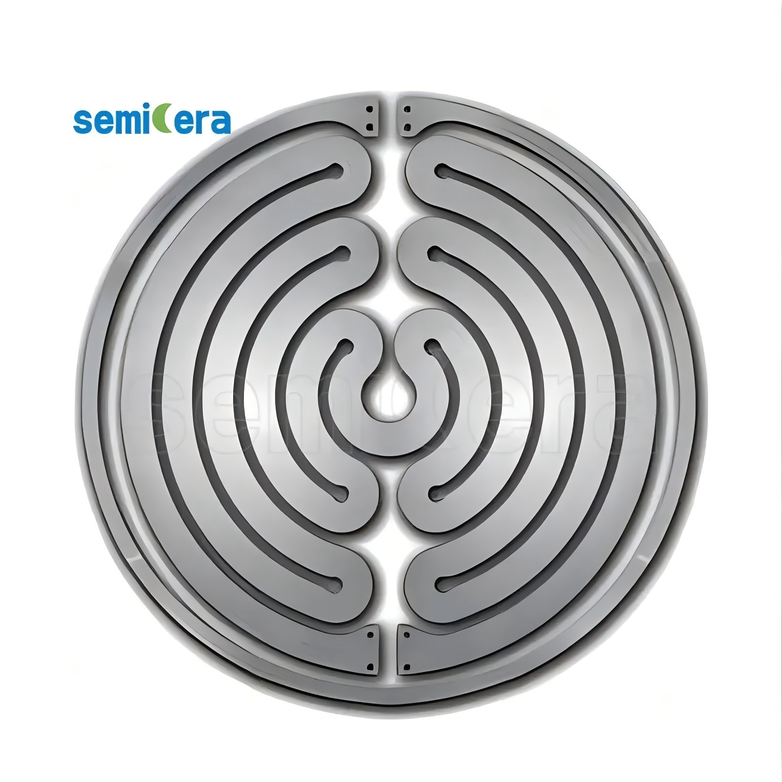
A wafer carrier is the point where the process chemistry meets a solid surface, and in MOCVD and plasma etch that single contact point governs more of the usable process window than the part number implies. Two carrier families are routinely compared during early sourcing: a CVD TaC-coated graphite carrier, where a thin tantalum carbide layer sits on a machined graphite body, and a solid CVD SiC component, where the entire part is bulk silicon carbide with no substrate beneath it.
They are not two versions of the same item. Published specifications assign them to different process steps, describe them with different metrics, and leave different failure modes for the buyer to manage. This comparison puts the documented figures side by side, scores each option against the criteria that matter at the research stage, and states plainly where each one stops.
Why carrier material is a process decision, not a part number
Semiconductors are materials such as silicon with tunable electrical conductivity, and they form the base for most electronics and integrated circuits. A carrier does not alter that base material, but it controls the environment around it: how evenly heat reaches the wafer, what happens chemically at the wafer edge, and how many particles the surface contributes to the chamber.
For procurement teams, the practical consequence is that carrier selection cannot be reduced to one headline figure. A 2200°C ceiling, a 25–45 µm coating, a density of at least 3.21 g/cm³ and an erosion rate below 2 nm/min are not competing claims about the same property. They describe different parts of the same decision, and comparing them directly without a frame is where most early-stage evaluations go wrong.
Two architectures, one comparison frame
Coated graphite: a graphite body with a CVD surface
In a coated carrier, the graphite body carries the geometry, the thermal path and the machinability, while the CVD coating carries the chemistry. Semicera's high-purity isostatic graphite is documented with an ultra-fine grain size of 2–5 µm, ash content at or below 5 ppm on the semiconductor ultra-pure grade, flexural strength of 45–65 MPa, and a coefficient of thermal expansion of 4.0–4.6 × 10⁻⁶ K⁻¹.
Two coating chemistries appear in the same portfolio. The CVD TaC-coated graphite carrier (model CVD-02) uses a cubic tantalum carbide matrix on a CVD SiC plus graphite structure, with a typical coating thickness of 25–45 µm, a maximum operating temperature up to 2200°C, and documented resistance to ammonia (NH3) and hydrogen (H2) etching. The CVD SiC-coated graphite carrier (model CVD-01) runs a thicker coating, typically 100 µm within a 50–150 µm range, at a purity level of 99.99995 percent, a coating hardness of 2500 Vickers, and an FCC beta-phase polycrystalline structure with (111) orientation.
Solid CVD SiC: no interface at all
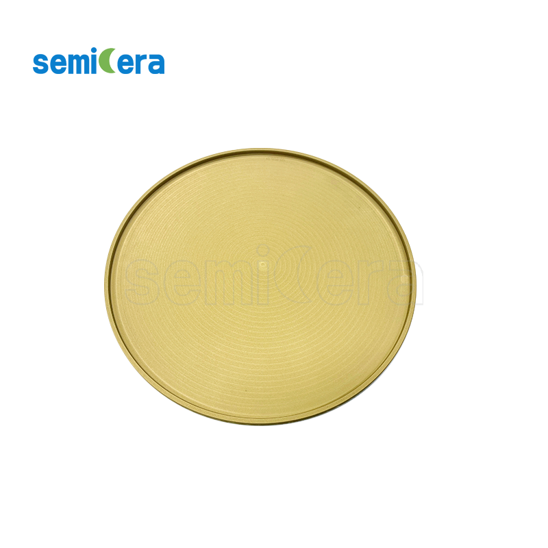
The solid CVD SiC part (model CVD-03) is a bulk silicon carbide process component or dummy wafer made from 100 percent bulk solid CVD SiC with zero substrate. It is documented at a material density of at least 3.21 g/cm³, 0 percent porosity, and thermal conductivity of at least 150 W/m·K. There is no coating-to-substrate boundary, so there is no coating adhesion failure mode to qualify.
The etch ring: a geometry-critical variant
The etch ring is a focus ring or edge ring for plasma etchers, based on either pure CVD solid SiC or high-purity silicon single crystal. Its published metrics are total metal impurity below 5 ppb, flatness tolerance of 10 µm or better, and a plasma erosion rate below 2 nm/min under high-density CF4/O2 plasma. These are geometry and contamination specifications rather than temperature specifications, and that distinction matters when buyers compare it against a susceptor.
Five criteria that actually separate the options
Documented operating ceiling. Only the TaC-coated carrier carries an explicit high-temperature figure in the published data, at up to 2200°C. The solid CVD SiC part and the etch ring do not publish a comparable ceiling, which does not mean they are lower — it means the number is not part of their stated specification set.
Process chemistry: NH3 and H2 versus fluorine and chlorine. The TaC-coated carrier is documented for outstanding resistance to ammonia and hydrogen etching, the gases that dominate group III-V epitaxy. The solid CVD SiC part is documented for high-density fluorine and chlorine plasma exposure in chamber positions. These are different chemical environments, and a result in one does not transfer to the other.
What thickness and density each measure. A coating thickness figure, 25–45 µm for TaC, describes how much process-facing material exists before the graphite body is exposed. A density figure, at least 3.21 g/cm³ with 0 percent porosity for bulk CVD SiC, describes the absence of open volume that could trap gas or shed particles. They are not alternative ways of stating the same quality.
Metallic purity. The etch ring publishes total metal impurity below 5 ppb. The carrier specifications publish coating purity, such as the 99.99995 percent figure on the SiC-coated carrier, and the underlying graphite at ash content at or below 5 ppm. Buyers should note which layer the purity number refers to.
Geometry and coating integrity. The etch ring publishes flatness at 10 µm or better, which is a direct statement about the plasma sheath boundary at the wafer edge. Coated carriers publish dimensional tolerance and, in the SiC-coated specification, an explicit requirement of no coating peeling under thermal cycling. Both are qualification items that a datasheet alone cannot close.
Buyer's scoring table
The table below compares the three options on the criteria above. Cells marked as not stated reflect the published specification set rather than a performance judgement.
| Criterion | CVD TaC-coated graphite carrier (CVD-02) | Solid CVD SiC component (CVD-03) | CVD SiC etch ring |
|---|---|---|---|
| Documented process role | MOCVD multi-pocket wafer susceptor or tray for semiconductor epitaxy | Bulk SiC process component or dummy wafer; plasma-exposed chamber component | Focus ring or edge ring for plasma etchers |
| Material architecture | Cubic TaC matrix coating on CVD SiC plus graphite | 100 percent bulk solid CVD SiC, zero substrate | Pure CVD solid SiC or high-purity single crystal silicon base |
| Documented temperature ceiling | Up to 2200°C | Not stated in the published specification | Not stated in the published specification |
| NH3 / H2 resistance | Documented as outstanding | Not stated | Not stated |
| Fluorine / chlorine plasma | Not stated | Documented for high-density F/Cl plasma exposure | Erosion below 2 nm/min under high-density CF4/O2 |
| Thickness or density | Coating typically 25–45 µm | Density at least 3.21 g/cm³; porosity 0 percent | Not stated |
| Thermal conductivity | Not stated for this part | At least 150 W/m·K | Not stated |
| Metallic purity | Coating purity stated; body graphite ash at or below 5 ppm | Not stated as a ppb figure | Total metal impurity below 5 ppb |
| Geometry control | Dimensional tolerance stated; peeling under thermal cycling is a stated requirement | Not stated | Flatness 10 µm or better |
| Interface risk | Present: the coating is the process-facing surface | Absent: no substrate interface | Absent on the bulk SiC base |
| Best-fit process step | High-temperature MOCVD and SiC or GaN epitaxy | SiC crystal growth; plasma-exposed bulk components | RIE and ICP-RIE edge control |
| Depth of published metrics | Moderate: temperature, chemistry, thickness | Moderate: density, porosity, conductivity | High: three numeric metrics |
Reading the scores by process step
MOCVD and SiC or GaN epitaxy: the TaC-coated carrier
The CVD TaC-coated graphite carrier is specified for ultra-high temperature epitaxy, with a documented operating scenario in Taiwan at 1600–2200°C under aggressive NH3 and H2 reduction. The stated requirements for that application are a maximum temperature resistance up to 2200°C, extreme ammonia and hydrogen corrosion resistance, zero carbon outgassing, and a coefficient of thermal expansion matched to the graphite body. Load and unload are handled by semiconductor handling robots, and the part operates as a static or rotating wafer carrier.
Zero carbon outgassing deserves attention in evaluation, because it is a specification about what the carrier does not release, not about what it withstands. A carrier that survives the temperature but contributes carbon to the gas phase is a different risk profile from one that does not.
SiC crystal growth and plasma-exposed bulk parts: the solid CVD SiC component
The solid CVD SiC part is documented for SiC crystal growth and, in a separate application, for high-density fluorine and chlorine plasma bombardment in a fab environment, described with a typical deployment in South Korea. The stated requirements there are a 100 percent solid CVD SiC matrix, zero porosity, extreme plasma erosion resistance, ultra-low particle generation and high electrical conductivity.
This is where the zero-substrate argument becomes concrete. With no coating and no substrate, the part has no layer that can separate, and its 0 percent porosity leaves no open volume for process gas to enter. The relevant comparison against a coated carrier is therefore not hardness or temperature, but the absence of an interface.
Plasma etch edge control: the etch ring
The etch ring is documented for RF-induced reactive ion etching environments, typically in South Korea, operating as a sacrificial static ring that secures the wafer edge under continuous plasma bombardment. Its stated function is to protect chamber components, control plasma distribution, improve etching uniformity and reduce particle contamination. The supporting equipment is inductively coupled plasma etchers or RIE systems.
Three numbers carry the specification: metal impurity below 5 ppb, flatness at 10 µm or better, and erosion below 2 nm/min. Flatness is a direct geometric input to the plasma boundary at the wafer edge; the impurity figure bounds contamination; the erosion rate sets how quickly the ring geometry drifts in service and therefore how the replacement interval is planned.
The middle option: SiC-coated graphite
The CVD SiC-coated graphite carrier (CVD-01) sits between the two extremes and is worth including in any shortlist. It is documented for epitaxy and RTP processes, with a stated deployment in Germany under continuous air supply, and with requirements that include ultra-high purity at the 6N level, low particle generation, strict dimensional tolerance and no coating peeling under thermal cycling. Its coating is substantially thicker than the TaC coating, at a typical 100 µm within a 50–150 µm range, and its hardness is stated at 2500 Vickers.
Technical explanation: what the numbers actually measure
Coating thickness is a service allowance and a stress variable, not a purity statement. A 25–45 µm TaC coating defines how much process-facing material exists before the graphite body becomes the exposed surface, and it also influences how the coating behaves through thermal cycles. A 50–150 µm SiC coating does the same job with more material present. Thicker is not automatically better: the qualification question is whether the coating stays intact across the temperature cycles the tool actually runs.
Density and porosity describe the body, not the surface. A solid CVD SiC part at 3.21 g/cm³ or above with 0 percent porosity is fully dense, which removes open volume as a particle and gas-trap source and makes thermal conductivity of 150 W/m·K or more a bulk property rather than a coating property.
For the etch ring, the flatness figure and the erosion figure work together. Flatness of 10 µm or better defines the starting geometry at the wafer edge; erosion below 2 nm/min defines how that geometry changes under high-density CF4/O2 plasma. Neither number on its own tells a buyer how long the ring stays within tolerance, which is why replacement planning needs both.
Where each option stops: limits and boundaries
Coated graphite has a consumable surface. The TaC coating is typically 25–45 µm thick, and it is the layer that absorbs the process chemistry. If a process attacks that layer faster than the qualification assumed, the graphite body becomes the exposed material. Coating integrity under thermal cycling is a stated requirement rather than a given, which is why the SiC-coated specification explicitly lists no coating peeling under thermal cycling as a condition.
Solid CVD SiC has a narrower documented scope than its properties suggest. It carries no coating interface and no porosity, but its published application framing is SiC crystal growth and plasma or etch chamber components. It is not documented as an MOCVD ammonia and hydrogen susceptor, so it should not be treated as a drop-in replacement for a TaC carrier position without qualification on that specific process.
The etch ring numbers are chemistry-specific. The erosion rate below 2 nm/min is stated under high-density CF4/O2 plasma. It is not a general figure for every etch chemistry, and buyers evaluating a chlorine-heavy or mixed process should treat the published value as a starting point for their own qualification.
Specifications do not transfer across process steps. A 2200°C ceiling does not describe an etch ring, and a 5 ppb metal figure does not describe an MOCVD susceptor. The most common evaluation error is lifting a number from one part family and applying it to a carrier used in a different step.
Commercial terms are the visible gap. Publicly available price bands, minimum order quantities and lead times for coated graphite, bulk CVD SiC and etch rings were not available in the source material reviewed for this comparison. Cost comparison therefore has to be built from quotations rather than from published data.
Comparison with traditional quartz carriers
Quartz remains the reference point that many buyers carry into the evaluation, and the published figures show where it sits. A quartz wafer boat in GE214 or equivalent ultra-high purity fused quartz, with SiO2 purity at 99.99 percent or above and slot pitch tolerance within ±0.05 mm, is rated for continuous operation at 1150°C and short-term operation up to 1300°C. A quartz furnace tube is documented with hydroxyl content below 20 ppm, an outer diameter tolerance of ±1.0 percent or better, and a bubble- and inclusion-free surface.
Silicon carbide carriers extend that envelope. The SiC wafer boat is documented at a maximum working temperature up to 1600°C with zero structural deformation, thermal shock resistance allowing cycling from 1000°C to room temperature, and a service lifespan more than five times that of traditional quartz boats. The TaC-coated graphite carrier, at up to 2200°C, sits above both in documented temperature terms.
Semicera's position in this comparison
Semicera, established in 2015, designs and manufactures high-purity semiconductor materials and components from a 40,000 m² facility with dual research centers and three large-scale production bases, employing approximately 600 people. Its products are used across LED, IC integrated circuits, third-generation semiconductors, epitaxy, MOCVD, CVD and photovoltaic applications.
The relevant point for this comparison is portfolio coverage rather than a single part. The documented range includes CVD SiC coatings, TaC coatings, PyC coatings, silicon carbide ceramics, semiconductor graphite components, quartz components, carbon fiber composite materials, CFC materials, rigid and soft felt, furnace thermal field materials, wafer boats, susceptors, preheat rings and furnace tubes. Its stated flagship products include SiC-coated graphite susceptors, TaC-coated diversion rings, SiC wafer boats, semiconductor quartz parts, and high-purity graphite components with impurity levels below 5 ppm.
For a buyer, that coverage means the two architectures compared here can be evaluated inside one documentation set and one supplier relationship. It does not mean they are equivalent, and it does not shorten qualification: the specifications above are per part, and each part carries its own application framing, its own stated requirements, and its own failure mode. Company-level capability and part-level qualification are separate questions, and the second one decides whether a carrier works in a given chamber.
Market trend: why carrier specifications are tightening
Demand for artificial intelligence and machine learning is described as driving innovations in chip fabrication, in the Stanford Emerging Technology Review assessment of the semiconductor field. The interpretation for consumables is straightforward: tighter process windows place more weight on the consistency of every surface inside the chamber, including carriers, rings and liners.
Supply structure reinforces the same effect. The U.S. International Trade Administration country commercial guide for Taiwan describes TSMC as dominating the foundry market, with U.S. firms such as Apple, NVIDIA and AMD relying heavily on it. Where device production concentrates, so does the qualification of process consumables, and a part that clears qualification at a high-volume fab tends to hold that position for a long time.
A data caveat belongs here. This review did not identify an eligible source with a transparent market definition for coated graphite, quartz and SiC component segments specifically, so segment sizing for these product families should be treated as an open gap rather than an established figure.
Future outlook
Three developments are worth tracking, each stated as an industry interpretation rather than a documented fact. First, as SiC substrates move to larger diameters and epitaxy runs hotter, the case for TaC-coated carriers in high-temperature positions strengthens, because the documented 2200°C ceiling and NH3/H2 resistance address exactly those conditions. Second, coating life management is likely to become a bigger part of total cost than coating price, which shifts evaluation toward thermal cycling evidence and refurbishment intervals. Third, documentation discipline will separate suppliers: buyers should expect per-part figures for temperature, chemistry, thickness or density, purity and geometry, and should be wary of a specification sheet that mixes them across process steps.
Frequently asked questions
What is the difference between a CVD TaC-coated graphite carrier and a solid CVD SiC component?
A CVD TaC-coated graphite carrier combines a machined graphite body with a thin cubic tantalum carbide coating, typically 25–45 µm, and is specified as an MOCVD multi-pocket wafer susceptor or tray for semiconductor epitaxy. A solid CVD SiC component is 100 percent bulk silicon carbide with zero substrate, a density of at least 3.21 g/cm³, 0 percent porosity and thermal conductivity of at least 150 W/m·K, and is specified for SiC crystal growth and plasma-exposed chamber positions. The first manages chemistry at a surface layer; the second has no surface-to-substrate interface at all.
What operating temperature can a TaC-coated graphite MOCVD susceptor reach?
The published maximum operating temperature for the CVD TaC-coated graphite carrier is up to 2200°C. Its documented epitaxy scenario, typically in Taiwan, is described at 1600–2200°C under aggressive ammonia and hydrogen reduction, with stated requirements that include zero carbon outgassing and a coefficient of thermal expansion matched to the graphite body.
How thick is the TaC coating, and why does coating thickness matter?
The TaC coating on the CVD-02 carrier is typically 25–45 µm. Thickness defines how much process-facing material exists before the graphite body is exposed, and it also affects how the coating behaves through thermal cycles. It is not a purity metric and is not directly comparable to the density figure published for bulk CVD SiC parts.
Which metrics define a CVD SiC etch ring for plasma etch?
Three published metrics define it: total metal impurity below 5 ppb, flatness tolerance of 10 µm or better, and a plasma erosion rate below 2 nm/min under high-density CF4/O2 plasma. The base material is either pure CVD solid SiC or high-purity single crystal silicon. Its stated function is to protect chamber components, control plasma distribution, improve etching uniformity and reduce particle contamination in inductively coupled plasma or reactive ion etching systems.
Can a coated graphite carrier replace a solid CVD SiC part in an etch chamber?
The published specifications assign the two to different process steps. The TaC-coated carrier is specified for semiconductor epitaxy with documented ammonia and hydrogen resistance, while the etch ring is specified for etch processes under fluorine and chlorine plasma with a stated erosion rate. No published data in this comparison documents a TaC-coated graphite carrier under high-density fluorine and chlorine bombardment, so substitution would need to be qualified on the specific chamber rather than inferred from a temperature rating.
What are the main limitations of each option?
Coated graphite carries a consumable surface: the coating is thin, an interface exists, and no coating peeling under thermal cycling is a stated requirement rather than a guarantee. Solid CVD SiC has no coating interface, but its documented application framing is SiC crystal growth and plasma or etch components rather than MOCVD ammonia and hydrogen susceptors. The etch ring’s erosion figure is stated for high-density CF4/O2 plasma specifically. Across all three, published price, minimum order quantity and lead-time data were not available, so commercial comparison requires direct quotations.
For readers who want the underlying component data behind this comparison, Semicera publishes a product catalogue covering its CVD coating, graphite, quartz and hot-zone component ranges, available for download as a PDF: Semicera product catalogue.
Есть вопросы или нужны дополнительные детали?
Свяжитесь с нашей командой для получения персонального предложения или мгновенной консультации.
Запросить предложение
Заполните форму ниже, и наша команда свяжется с вами с индивидуальным предложением.
Прямой чат WhatsApp
Предпочитаете общаться в реальном времени? Напишите нам в WhatsApp для мгновенной помощи и быстрых ответов.
- Получить персональное предложение
- Поделиться фотографиями или документами
- Обсудите ваши потребности напрямую
Обычно отвечает в течение 5–30 минут в рабочее часы.