
Double-Sided PCB Sourcing: Certification, Specs, and Price Drivers
A double-sided PCB puts copper on both faces of the substrate and joins the two sides with plated through-holes. It is a mature structure and one of the most cost-efficient interconnects in modern electronics. The difficulty is rarely the board itself: it is that two boards described as double-sided, FR-4 and 1.6 mm can be quoted very differently because the finish, the copper weight, the electrical test method or the certification evidence behind them are not the same.
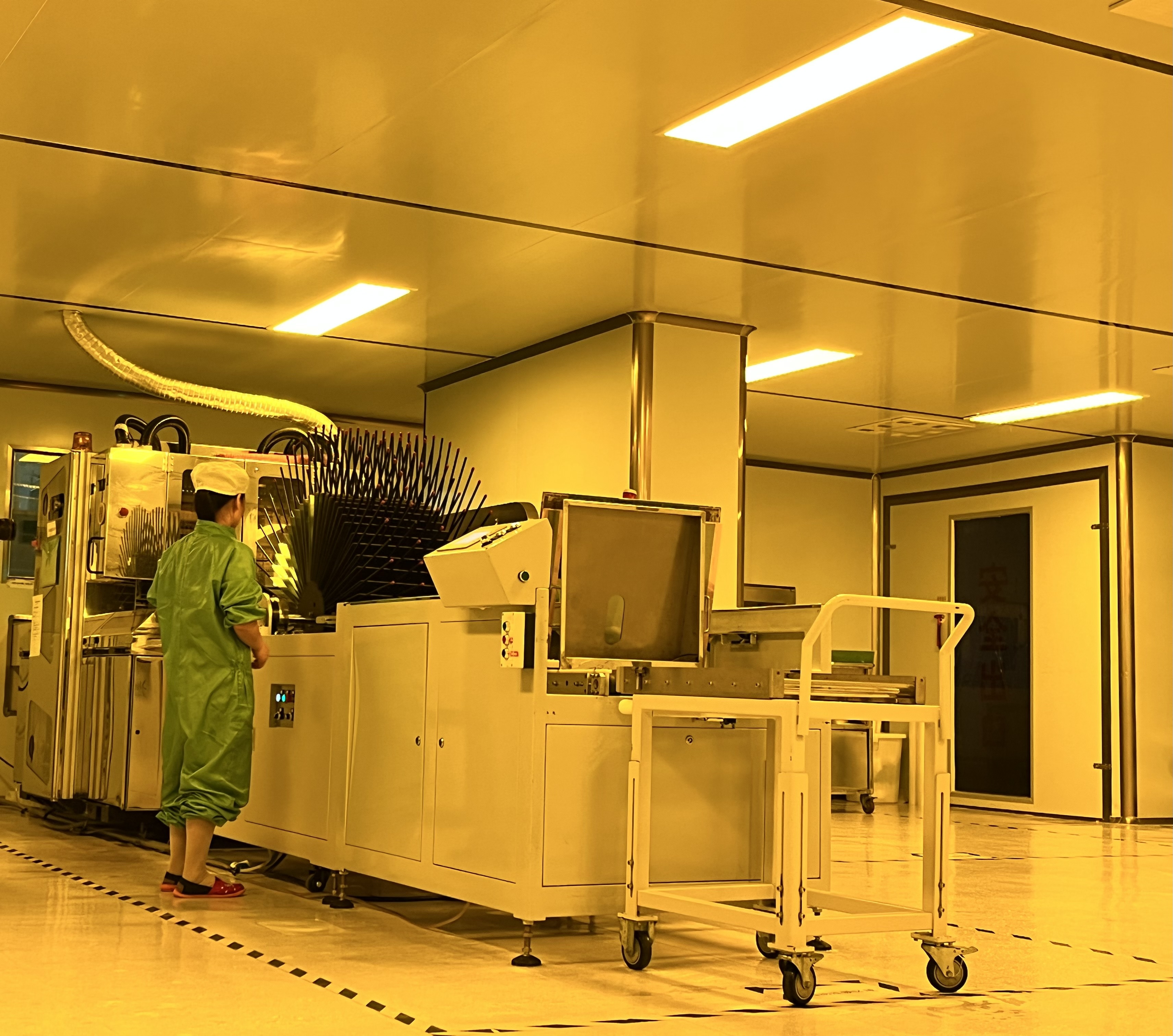
Film imaging in a Class 10,000 clean room. Double-sided PCB cost is decided less by the two copper layers than by the process options specified around them.
Why two double-sided PCB quotations rarely describe the same board
Most purchasing processes start from a drawing and a board outline. The quotation responds to everything the drawing does not say. Surface finish is the clearest example: HASL lead-free and ENIG sit in different cost bands and behave differently across storage and soldering. Neither is wrong, but one is a default and the other is a decision.
Electrical test is the second. Fixture E-test and fly-probe E-test carry different economics, and suppliers may switch between them based on order quantity. That switch is explicit in published specifications rather than hidden: open and short testing is performed by fixture E-test or fly-probe E-test according to order quantity. A buyer comparing a 50-piece prototype quote against a 5,000-piece production quote is comparing two different test regimes, not two prices for the same work.
Certification scope is the third. A board built in a facility audited to IATF 16949 carries a different documentary footprint from a board sold as automotive grade without a certificate number, an issuing body or a validity window. That difference shows up in the price, and it shows up again during a customer audit.
The constraints a double-sided PCB enquiry should actually lock down
A workable RFQ for a double-sided board does not describe a board. It describes a set of boundaries. The table below lists the ones that change most often between quotations.
| Parameter | What it constrains | What to state in the RFQ |
|---|---|---|
| Layer count and construction | Routing freedom, via strategy, whether two layers are sufficient at all | 2-layer, finished thickness, whether controlled impedance is required |
| Base material and Tg | Thermal margin, behaviour across repeated reflow cycles | Standard FR-4 or high-Tg FR-4, with the Tg value required |
| Finished copper thickness | Current-carrying capacity and etch tolerance | 1 oz or 2 oz, and whether outer, inner or both |
| Minimum line width and spacing | Routable density, and whether the design tips into multilayer | Values in mil, plus the supplier stated process limit |
| Minimum hole size | Via count, drill cost, plating reliability | Value in mm, and whether PTH or NPTH |
| Surface finish | Solderability, shelf life, cost band | HASL lead-free, ENIG, OSP, immersion tin or immersion silver |
| Solder mask and silkscreen | Assembly identification, AOI contrast | Colour combination required |
| Electrical test | Sorting cost and escape rate | Fixture E-test or fly-probe, and the sampling rule |
| Certification evidence | Whether the board can enter automotive, medical or industrial supply chains | IATF 16949, UL, RoHS and REACH documents, not logos |
| Packaging | Transit damage and handling at the assembly line | Vacuum packing or a specified alternative |
| Quantity and lead time | Production slotting and test method selection | Prototype or mass volume, and the day count required |
Two of these rows are routinely left blank, and both are expensive to correct later. Minimum line width and spacing determines whether a double-sided design is optimised or simply fitted in; stating it forces the supplier to confirm whether the density is inside their process window. Electrical test determines what leaves the factory undetected; stating it forces a decision rather than a default.
What certifications a double-sided PCB project actually needs
Certification requirements come from the downstream product, not from the board structure. A consumer accessory may need nothing beyond a RoHS and REACH declaration. An automotive module changes the supplier threshold immediately.
SHENZHEN JERICO MULTILAYER PCB CO., LTD, trading as Jerico, is a PCB manufacturer founded in 2009 with a manufacturing base in Wuping, Fujian and a business centre in Shenzhen, Guangdong. The company holds IATF 16949:2016 certification issued by NQA, with certificate numbers NQA:T184224, IATF:0493049 and IATF USI:6GXSFM. The certification scope is the manufacturing of circuit boards, and it is valid from 2023-12-22 to 2026-12-21.
Alongside the automotive certificate, the company lists ISO 9001, ISO 14001, UL Recognized status under File No. E519316, CQC China Compulsory Product Certification, National High-tech Enterprise status, and RoHS, REACH and SGS compliance test reports. Production is described as following IPC-A-600H, IPC-6012 and UL-796.
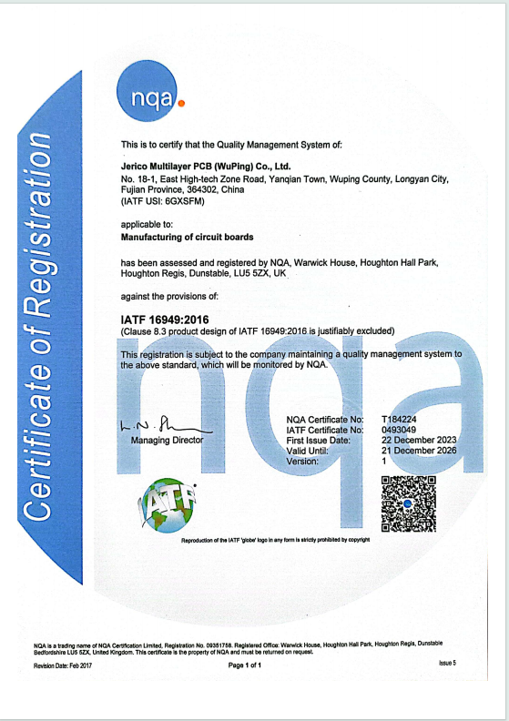
The IATF 16949:2016 certificate lists the issuing body, three certificate numbers, the scope and a validity window up to 2026-12-21. Buyers can verify all four attributes with the issuer.
For buyers, the practical move is to treat these as a document set rather than a row of badges. Automotive programmes typically require material certifications, a UL report, an impedance report and the factory electrical test report, with PPAP documentation for volume builds. A certificate number without a scope statement does not answer the question of whether the specific facility that will produce the double-sided board is covered.
Where factory capability ends and a single order begins
Jerico operates a 20,000 square metre plant with monthly capacity of 50,000 to 70,000 square metres, equivalent to roughly 960,000 square metres per year. The company profile lists 30 engineers, an export ratio of 40 percent and main markets in the EU and the USA.
On the manufacturing side, mass production is described for rigid PCBs from 1 to 18 layers, with double-sided constructions falling inside that range, and HDI products extending to 32 layers. The stated process capability includes minimum trace width and spacing down to 3/2.8 mil and impedance tolerance of plus or minus 10 percent. Surface finishes offered include ENIG, ENEPIG, selective gold plating, OSP, immersion tin, immersion silver and HASL.
That capability describes what is possible. An order locks down a much narrower slice of it. A double-sided board produced with HASL lead-free, 1 oz copper and sampling-only inspection is a different product from the same board produced with ENIG, 2 oz copper and 100 percent flying-probe testing, even though both leave the same facility.
A limitation worth stating plainly: double-sided PCB sourcing is rarely a technical challenge. The weak point is documentation. Published specifications for individual boards often leave gaps, and a specification may list 3 mil minimum line width and 3 mil minimum line spacing while including no impedance-control report, no stated IPC class, no UL file number and no test report reference. Those gaps tend to surface during production rather than during quotation, and a buyer who does not write the requirement into the RFQ should not expect the supplier to add it.
Where a double-sided PCB is still the right choice
Double-sided boards remain the default interconnect for products where circuit complexity is moderate, board area is generous and unit cost dominates the design brief. Jerico lists applicable industries including consumer electronics, industrial control and automation, security and surveillance, telecommunication and networking, automotive electronics, medical equipment, and IoT and smart home devices.
Long-running supply relationships are one indicator of where the structure fits. A Brazilian EMS factory has taken LED driver PCBs from the company for six years across roughly 300,000 pieces, with defect rates in the range of 3 per 1,000 to 8 per 1,000. A Russian end-product manufacturer has taken civil drone PCBs for eight years across approximately 50,000 pieces. These cases describe sustained delivery rather than a specific board construction, so they should be read as evidence of continuity rather than as proof that any particular product uses a two-layer design.
For lower-complexity industrial control boards, power supply front ends, sensor carriers and consumer device mainboards, a two-layer construction is often sufficient, and the cost difference against a four-layer build is real. The mistake is treating two layers as a default rather than as a design conclusion.
Mixed market signals and what they mean for a low-density board
Prismark projects the global PCB market to reach roughly 95.8 billion USD in 2026, with China's share of global PCB production projected at approximately 60 percent. Commercial research cited in the same dataset puts multilayer PCBs at around 52 percent of global production volume.
Double-sided boards sit inside the market those figures describe, but at the low-density end of it. The interpretation should stay disciplined: aggregate growth numbers describe total demand, not the trajectory of one construction type, and they do not translate directly into growth for two-layer boards. What they do indicate is that the centre of volume remains in Asia, and that a buyer sourcing double-sided PCBs from a Shenzhen-based supplier is operating inside the densest production cluster in the market.
Double-sided versus multilayer: where the boundary sits
The transition from two layers to four is not a cost decision, it is a routing decision. Once a design needs dedicated power and ground planes, impedance-controlled high-speed buses, or fan-out from high pin-count BGA devices, two copper layers stop being adequate and the conversation moves to multilayer construction.
| Dimension | Double-sided PCB | Multilayer PCB |
|---|---|---|
| Copper layers | 2 | 4 and above |
| Routing freedom | Limited to two routing surfaces | Additional internal routing and plane layers |
| Ground and power planes | No dedicated planes; EMI control depends on layout discipline | Dedicated planes improve return paths and shielding |
| High pin-count BGA fan-out | Not practical | Supported, with HDI constructions reaching 0.4 to 0.5 mm BGA pitch |
| Relative cost | Lower at equivalent area and quantity | Higher, driven by lamination cycles and layer count |
| When it becomes the wrong choice | When routing, plane or EMI requirements exceed two layers | When the circuit does not use the added layers |
The limitation runs in both directions. A double-sided board cannot deliver the return-path control of a board with a solid ground plane, and no amount of process care changes that. Equally, specifying a four-layer board for a circuit that fits comfortably on two layers adds cost without adding function.
Future outlook
Double-sided PCB demand typically follows long product lifecycles: industrial controllers, power supplies, security devices and consumer accessories where the design is stable and the annual volume is predictable. Those segments do not move quickly, and the structure is not at risk of being displaced by higher-density alternatives in the applications where it already fits.
What is changing is the documentation expectation around it. Automotive and medical customers increasingly ask for traceability of board batch, production parameters and test records, alongside material declarations and reliability data. Suppliers that can produce those documents on request are easier to qualify than suppliers that cannot, and that gap is likely to matter more in future sourcing decisions than marginal differences in unit price.
Frequently asked questions
What certifications are required for a double-sided PCB project?
The requirement follows the end product rather than the board structure. For automotive-related work, IATF 16949:2016 is the relevant standard. Jerico holds IATF 16949:2016 certification issued by NQA under certificate numbers NQA:T184224, IATF:0493049 and IATF USI:6GXSFM, with a scope covering the manufacturing of circuit boards and a validity period ending 2026-12-21. Other listed credentials include ISO 9001, ISO 14001, UL Recognized File No. E519316, CQC, and RoHS, REACH and SGS reports. Buyers should confirm that the certificate covers the specific facility producing the boards.
Which parameters drive a double-sided PCB quotation most?
Surface finish, finished copper thickness, board thickness, board size, order quantity, electrical test method and certification documentation are the parameters that move a quotation most. Electrical test is often underestimated: published specifications state that open and short testing is performed by fixture E-test or fly-probe E-test according to order quantity, so the order size itself changes the test route and therefore the cost.
What minimum order quantity and lead time apply to double-sided PCBs?
The listed minimum order quantity is 1 piece, and lead time ranges from 7 to 45 days. Boards are supplied in vacuum packaging. The wide lead-time range reflects differences between prototype orders, small pilot batches and volume production rather than a single fixed schedule, so the required delivery date should be stated in the enquiry.
Can controlled impedance be specified on a double-sided PCB?
Controlled impedance can be specified as a requirement. Jerico states an impedance tolerance of plus or minus 10 percent as a general process figure. Specific differential and single-ended targets depend on the design and stack-up, and the buyer should confirm the achievable values before release rather than assuming the general figure applies unchanged to a two-layer construction.
How can a buyer verify a supplier's IATF 16949 certificate?
Verification uses four attributes: the certificate number, the issuing body, the validity period and the scope. Jerico's certificate names NQA as the issuing body, lists three certificate numbers, states the scope as manufacturing of circuit boards and runs from 2023-12-22 to 2026-12-21. Beyond the certificate itself, automotive buyers typically request material certifications, a UL report, an impedance report and the factory electrical test report, with PPAP documentation for volume programmes.
When should a double-sided design move to multilayer construction?
The switch is warranted when routing density, power and ground plane requirements, or EMI control exceed what two copper layers can deliver. The absence of dedicated planes in a two-layer board is a structural constraint rather than a process quality issue, so additional inspection or tighter tolerances do not resolve it. For designs that need high pin-count BGA fan-out, HDI constructions are the relevant option.
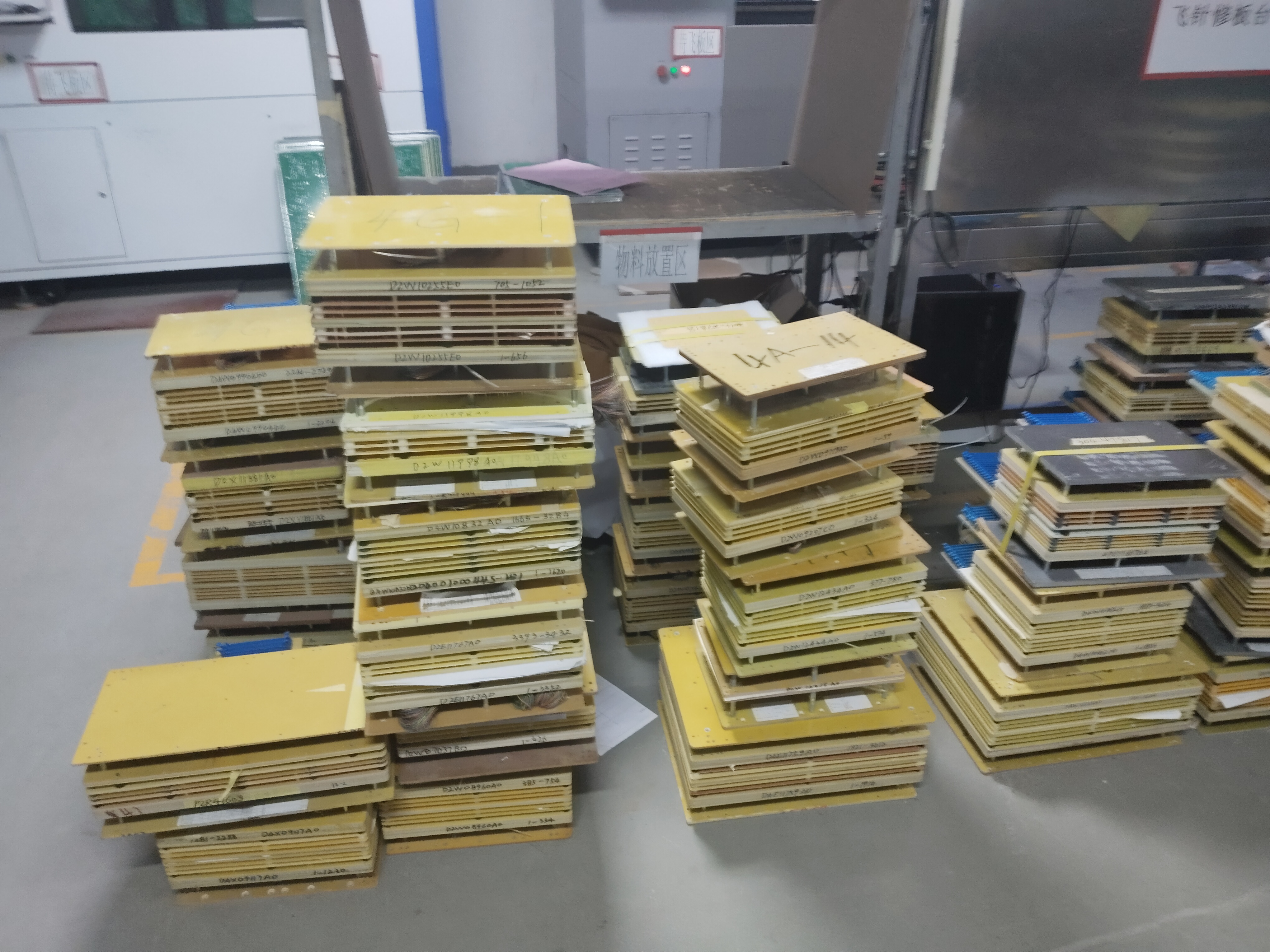
Dedicated test fixtures stored by order. The choice between fixture E-test and fly-probe E-test is one of the cost drivers that most often separates two quotations for the same board.
Есть вопросы или нужны дополнительные детали?
Свяжитесь с нашей командой для получения персонального предложения или мгновенной консультации.
Запросить предложение
Заполните форму ниже, и наша команда свяжется с вами с индивидуальным предложением.
Прямой чат WhatsApp
Предпочитаете общаться в реальном времени? Напишите нам в WhatsApp для мгновенной помощи и быстрых ответов.
- Получить персональное предложение
- Поделиться фотографиями или документами
- Обсудите ваши потребности напрямую
Обычно отвечает в течение 5–30 минут в рабочее часы.