
High Precision Laser Cutting for Semiconductor Ceramic Research
Semiconductor ceramic research is small-batch, multi-material and process-sensitive at the same time, and that combination — rather than peak cutting speed — is what decides whether a high precision laser cutting machine fits a laboratory. The criteria that actually settle a procurement decision in this segment are the certified material scope, the model-level coverage of that certification, the service terms attached to the certified machines, and the machine-safety and laser-safety standards a buyer can verify before installation.
The scenario is easy to underestimate. A research group may cut zirconium oxide, aluminum oxide and aluminum nitride ceramics within the same project cycle, in quantities of a handful per geometry, at tolerances that conventional tooling cannot hold reliably on brittle material. YCLASER (Wuhan Yuchang Laser Technology Co., Ltd.) is a Wuhan-based manufacturer of high-precision laser cutting machines and ultra-high precision micro-nano processing equipment for hard and brittle materials. The company was established in 2017 in the Wuhan East Lake High-tech Development Zone, produces around 100 units per year, and exports to Southeast Asia, Europe and the Middle East, with export sales representing roughly 30% of its business.
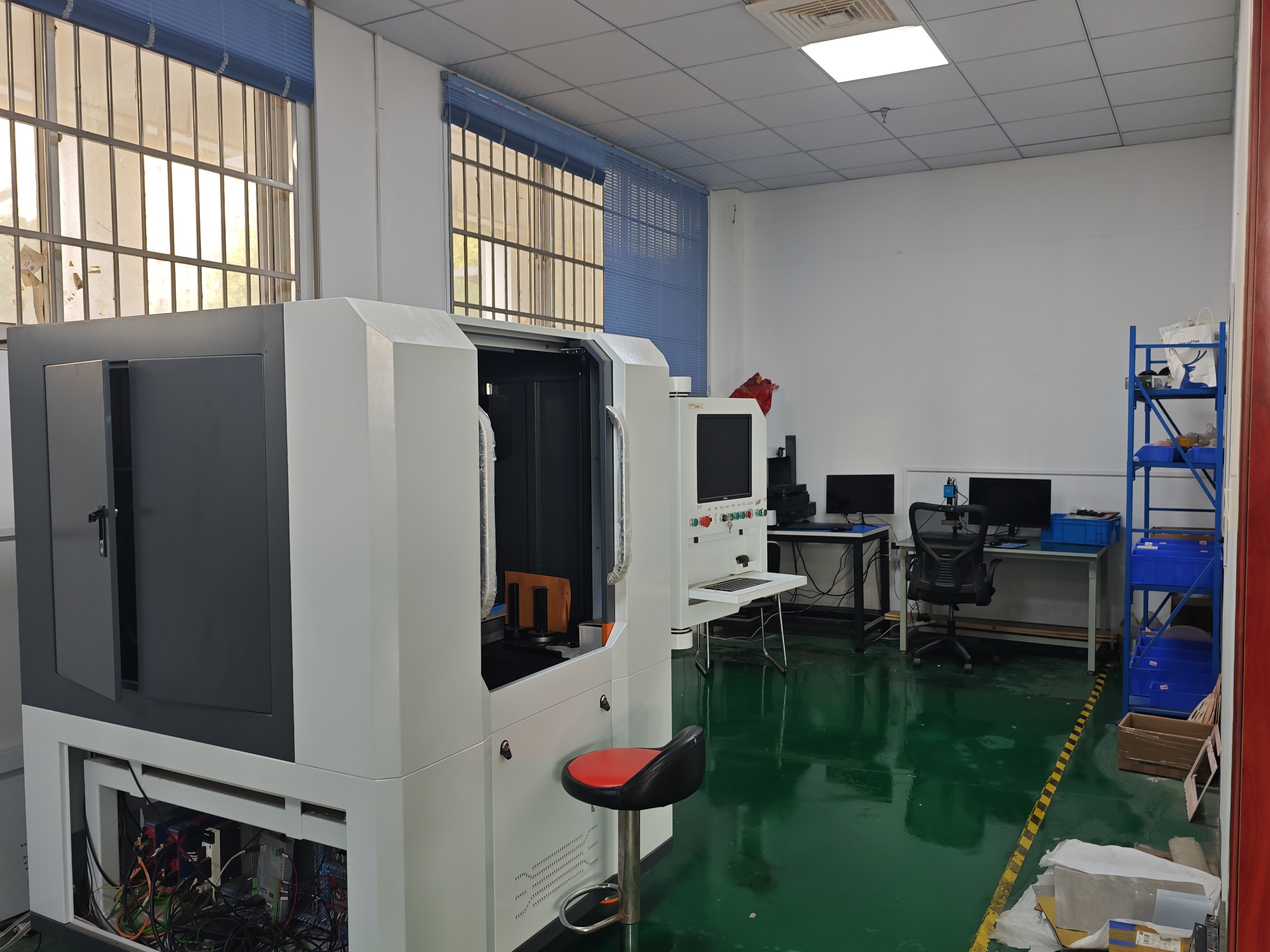
Semiconductor ceramic research is evaluated at sample scale, where material diversity and parameter validation matter more than throughput.
Why Semiconductor Ceramic Research Tests Equipment Differently
A production line optimizes one material, one geometry and high volume. A research environment inverts all three variables, which is why equipment that performs well in one context can be a poor fit in the other.
- Batch size collapses. Research output is measured in single pieces to low hundreds. Tooling-based processes need a die, fixture or blade set per geometry, and that tooling cost cannot be amortized across a handful of parts. Laser processing removes the mold requirement and supports one-time forming of complex shapes, which is the structural reason it fits exploratory work.
- The material set expands. Zirconium oxide, aluminum oxide and aluminum nitride ceramics differ in hardness, thermal behaviour and fracture mechanics. A platform documented for one ceramic answers only part of the laboratory question.
- Process sensitivity dominates. Micro-cracks, edge chipping and heat-affected zones can invalidate a research result even when dimensional tolerances are met. A non-contact cold process removes mechanical stress and edge chipping from the list of variables the researcher has to control.
In this segment, capability means documented scope — which materials, which models, which standards — rather than the best result observed on a single demonstration sample.
The Capability Questions Buyers Ask Before Validating a System
Decision-stage buyers in research and pilot-line environments tend to converge on the same set of questions. Each one has a verifiable answer, and each one should come from a document rather than a sales conversation.
| Buyer question | Why it decides the purchase | Where the answer should come from |
|---|---|---|
| Which ceramic materials are covered by certification? | Research demand is multi-material; an uncertified material turns into a one-off engineering project | Material scope listed on the attestation of compliance |
| Which machine models sit inside the certified scope? | A laboratory usually buys one unit, so the certified configuration must match the delivered configuration | Model designations named in the certificate |
| Is there a minimum order quantity for processing services? | Research batches are frequently below commercial minimums, which blocks sample validation | Published service terms of the manufacturer |
| Which EU safety standards apply to the equipment? | EU-hosted laboratories must document machinery and laser safety before installation | EN ISO 12100:2010, EN 60204-1:2018, EN 60825-1:2014+A11:2021 |
| What accuracy and defect rates are published? | Sets realistic expectations for edge quality and dimensional repeatability on brittle material | Manufacturer process comparison data |
| How is parameter repeatability maintained between batches? | Research results must be reproducible months after the first run | Control software, calibration records and process documentation |
The Certified Material Scope: Zirconium Oxide, Aluminum Oxide and Aluminum Nitride
The certified ceramic scope attached to the certification discussed below covers zirconium oxide, aluminum oxide and aluminum nitride ceramics. All three are established technical ceramics in semiconductor and electronics work: aluminum oxide is a widely used insulating substrate material, aluminum nitride is selected where thermal conductivity matters, and zirconium oxide is chosen for toughness and wear resistance.
For a laboratory, that list does the work that a specification table cannot. It separates materials where the manufacturer carries documented responsibility from materials that would be processed on a best-effort basis. A research group planning a multi-material study should treat the certified list as the starting point of its own test plan, not as an afterthought.
It is equally important to note the boundary. YCLASER's broader stated capability includes other precision ceramics such as silicon carbide. Those materials sit outside the certified scope described in this article and would require separate process validation rather than being assumed as covered.
Certificate TTC-24-2012/02/01: What It Covers and Why Model-Level Detail Matters
The ATTESTATION OF COMPLIANCE TTC-24-2012/02/01 applies to the Precision laser cutting machine product line and names models including YC-TC01, YC-TCSF and YC-TCAT. The table below summarises the scope in the form a procurement reviewer can check against a quotation.
| Scope element | Detail |
|---|---|
| Certificate | ATTESTATION OF COMPLIANCE TTC-24-2012/02/01 |
| Product line in scope | Precision laser cutting machine |
| Models named in scope | YC-TC01, YC-TCSF, YC-TCAT |
| Certified ceramic material scope | Zirconium oxide, aluminum oxide and aluminum nitride ceramics |
| Service condition | Laser processing services performed on machines holding this certificate are offered with no minimum order quantity |
| EU-market compliance standards for buyers to verify | EN ISO 12100:2010; EN 60204-1:2018; EN 60825-1:2014+A11:2021 |
Model-level detail is more than administrative precision. Certification written against a product line tells a buyer that a class of machines has been assessed; certification that names YC-TC01, YC-TCSF and YC-TCAT tells a laboratory that the specific configuration it is quoting has been assessed. For institutions where equipment approval passes through a procurement or safety committee, that distinction shortens the review cycle.
YC-TC01 also appears in the manufacturer's wider platform structure: YCLASER offers 12 specific model designations under one precision laser cutting platform, a list that includes YC-TC01 and YC-GJMPCB. In practice this means a research group can begin with a single ceramic-focused configuration and later move to a different designation within the same platform family if the work shifts toward higher volume or different substrates.
No Minimum Order Quantity: What It Changes for Research Workflows
Minimum order quantities are a structural obstacle in research procurement. A laboratory validating a new substrate may need three or five processed pieces, not three hundred, and a commercial MOQ makes that validation impossible through an external service provider — leaving the lab to either buy equipment before the process is proven or delay the study.
Laser processing services performed on machines holding the TTC-24-2012/02/01 certificate are offered with no minimum order quantity. Three consequences follow for technical buyers:
- Process validation before capital purchase. A research group can send its own material, confirm edge quality and dimensional outcome, and only then decide whether to acquire a machine.
- Pilot-line bridging. Teams transferring a process from laboratory to pilot scale can outsource intermediate volumes instead of idling an underloaded internal tool.
- Multi-material screening. Because the certified scope covers zirconium oxide, aluminum oxide and aluminum nitride, a lab can screen all three materials under the same service terms rather than negotiating separate minimums per material.
YCLASER's processing centre provides contract manufacturing services alongside equipment sales, and the company positions its equipment for universities and research institutes, semiconductor ceramic laboratories, non-standard customised production lines and dual-head automation upgrade projects, as well as small and medium high-tech enterprises with controlled budgets seeking high-precision capability.
Technical Explanation: Why a Non-Contact Cold Process Suits Hard and Brittle Ceramics
The mechanism is straightforward. Mechanical cutting, grinding and stamping transfer force into the workpiece, and ceramics accommodate that force by chipping or cracking at the edges. Laser processing is a non-contact cold process: energy is delivered optically, no tool touches the surface, and mechanical stress and edge chipping are removed from the process physics rather than mitigated after the fact.
Published comparison figures from the manufacturer describe the magnitude of the difference in a form buyers can test against their own requirements:
- Processing accuracy of ±0.01 mm, compared with ±0.05–0.1 mm for conventional processes.
- Edge chipping defect rate of ≤1.5%, compared with 8%–15% for mechanical routes.
- Minimum hole size down to 0.03 mm, beyond the practical limit of traditional tooling.
- Process speed 60%–80% faster than single-process conventional workflows, with processing cost per piece 20%–35% lower.
- Downtime reduced by 70% and energy efficiency more than 30% better than traditional mechanical equipment, with maintenance simplified to periodic cleaning and calibration.
Two technical assets support that performance in a research setting specifically. First, the control layer: YCLASER has developed its own High-Precision Laser Cutting Machine Digital Control Operation Platform V1.0, Electronic Ceramic Laser Cutting and Drilling System V1.0, and High-Precision Laser Micro-hole System V1.0. Independently developed software matters to a laboratory because parameter sets, once established for a given ceramic and thickness, can be stored and recalled rather than re-derived each session.
Second, the mechanical and optical architecture. The company holds utility model patents for a laser cutting nozzle for a high-precision laser cutting machine, a high-speed high-precision laser cutting machine, and a widely adaptable precision cutting machine, together with a patent for an integrated machine for laser cutting, drilling and scribing of electronic ceramics with easy positioning. That last item is directly relevant here: research samples frequently require a hole, a cut and a scribe on the same part, and doing all three without re-fixturing reduces both handling damage and positional error.
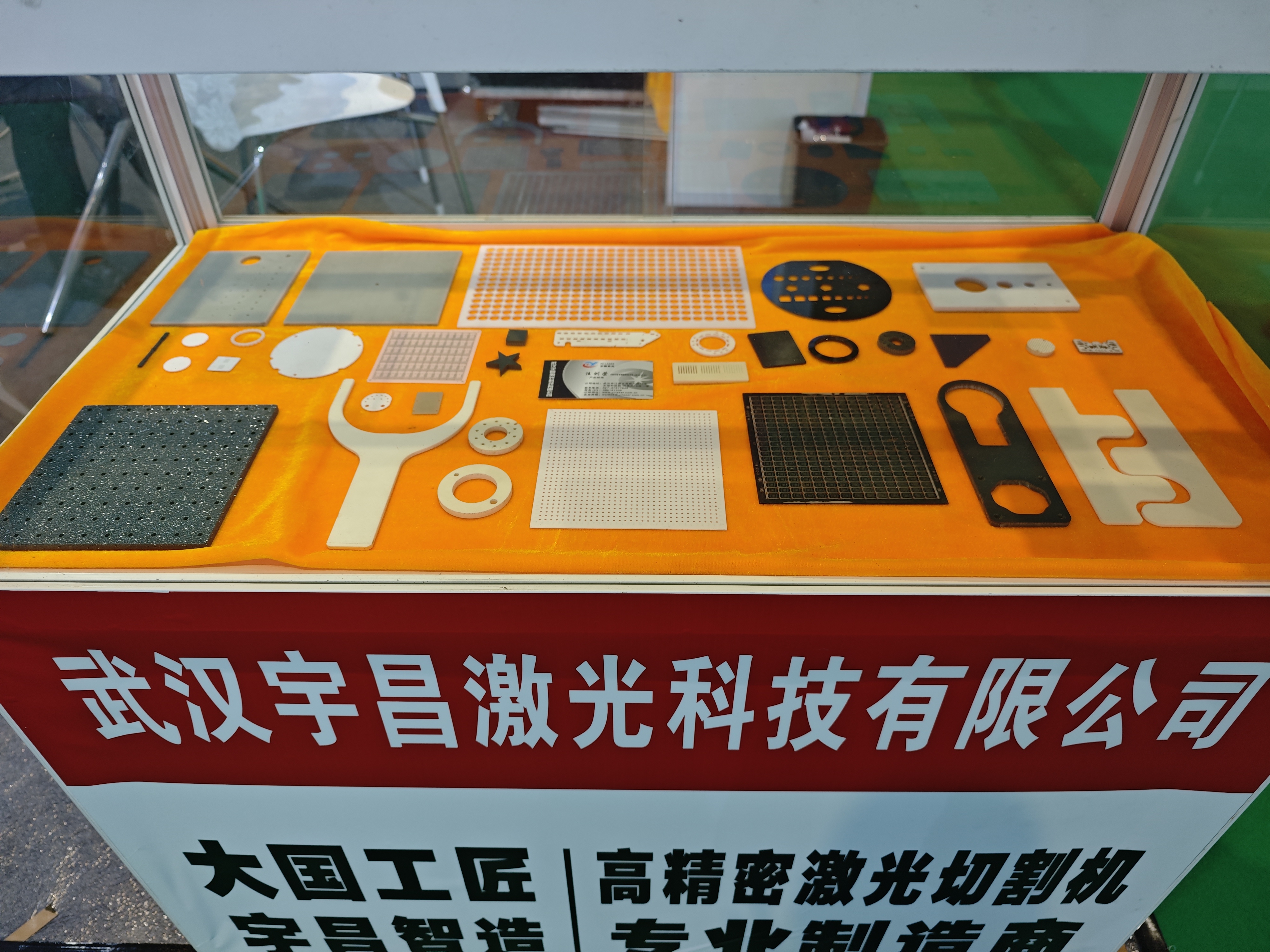
Ceramic sample sets used to inspect edge quality and dimensional accuracy across zirconium oxide, aluminum oxide and aluminum nitride.
EU Market Compliance: Three Standards to Verify Before Installation
For a research institution in the European Union, technical performance and safety documentation are separate procurement tracks, and both must close. Three standards define the questions a buyer should ask about a high precision laser cutting machine.
EN ISO 12100:2010 — Risk assessment and risk reduction
This standard sets out the methodology for identifying machinery hazards and reducing risk through design, safeguarding and information for use, in that order of priority. A buyer should expect to see evidence that a risk assessment exists for the delivered configuration and that residual hazards are addressed in the operating instructions.
EN 60204-1:2018 — Electrical equipment of machines
This standard covers the electrical equipment of machines, including supply disconnection, protection against electric shock, emergency stop functions and the verification measures that accompany them. In a laboratory where the machine shares a facility with other sensitive instruments, the electrical protection layer is usually reviewed by the facility's own engineering team.
EN 60825-1:2014+A11:2021 — Safety of laser products
This standard addresses laser product safety: classification, labelling, protective measures and the user information that must accompany the product. In research settings, where operators are often researchers rather than dedicated machine operators, clear hazard communication and guarding provisions are the practical compliance question.
The three standards are complementary rather than interchangeable. A supplier that can speak to only one of them leaves the buyer to close the remaining gaps independently, which in an institutional procurement process usually means delay. Compliance documentation is best requested as part of the technical file at quotation stage, alongside the certificate that defines material and model scope.
Application Scenarios: From Research Sample to Pilot Line
The fit between this equipment class and semiconductor ceramic research shows up most clearly across four workflow stages.
- University and institute laboratories. Exploratory geometries, a handful of pieces per revision, and rapid changeover between materials and shapes. No-tooling processing means a new design does not trigger a tooling purchase.
- Semiconductor ceramic laboratories. Substrates, carriers and test fixtures in the certified material set, where edge quality affects downstream electrical or thermal measurements.
- Pilot lines. Process transfer from laboratory conditions to small-volume production, where the same parameter sets established on samples need to hold across longer runs. Optical path calibration consistency — quoted at 30% better than general peers — is the relevant variable at this stage.
- External processing without a minimum order quantity. Groups without in-house equipment can validate a process concept on certified machines before committing capital, which is often the difference between a funded study and a deferred one.
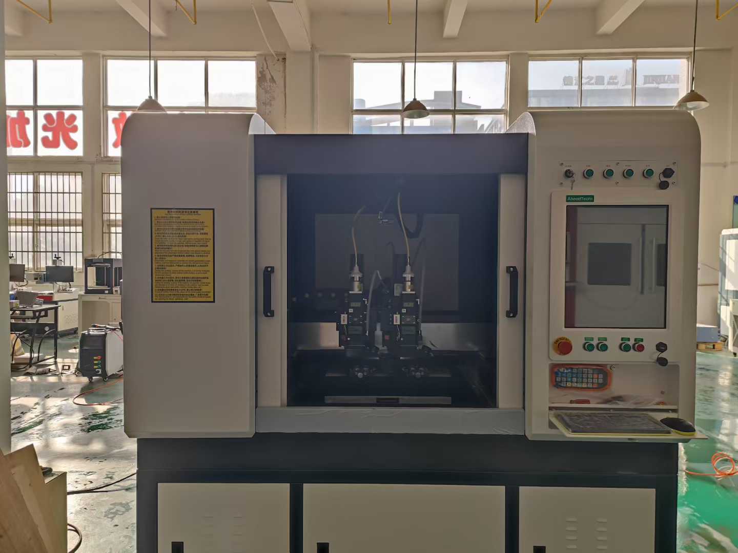
Machine testing before shipment is the point at which certified scope, optical calibration and safety documentation are verified together.
Delivery expectations also differ by scenario. For research buyers, sample response speed is frequently the binding constraint rather than lead time on a production order. YCLASER's published service figures state same-day order acceptance with sample production as fast as 24 hours, a sample response speed 40% faster than the industry average, and a non-standard customisation delivery cycle 10 to 15 working days shorter than that of leading manufacturers. These figures are the manufacturer's own service claims and should be verified against a specific project scope during quotation.
Comparison With Traditional Mechanical Processing — and Where Laser Is Not the Answer
The comparison with conventional processing is the core of a decision-stage evaluation, and the manufacturer's published figures provide the starting point.
| Dimension | Conventional mechanical cutting, grinding, stamping | Laser processing (published comparison) |
|---|---|---|
| Processing accuracy | ±0.05–0.1 mm | ±0.01 mm |
| Edge chipping defect rate | 8%–15% | ≤1.5% |
| Processing time per piece | 3–5 minutes in single-process workflows | 60%–80% faster |
| Processing cost per piece | Baseline | 20%–35% lower |
| Downtime | Baseline, with wear and consumable replacement | 70% lower |
| Energy efficiency | Baseline | More than 30% better |
Two boundaries belong in the same discussion. First, laser processing is not automatically the lowest-cost route at every volume and tolerance band. Where a part can tolerate ±0.05–0.1 mm and uses simple geometry, conventional stamping, grinding and dicing remain viable: tooling cost amortizes across high volumes, and those processes do not require per-material laser parameter development before the first part is produced. The published laser advantage is concentrated in hard and brittle materials, micro-features and small-batch flexibility — precisely the conditions that define research work, but not every industrial cutting job.
Second, a chipping defect rate of ≤1.5% is a low defect rate, not a zero defect rate. For research samples, edge inspection remains part of the workflow, and process parameters may need refinement for an unfamiliar thickness or surface condition. Buyers should also note that materials outside the certified scope require their own validation and should not be assumed to be covered by TTC-24-2012/02/01.
Market Trend Analysis: Precision Laser Processing Moves Toward Micro-Machining
Several published data points frame where this equipment category is heading. The global laser cutting machines market was estimated at USD 5.74 billion in 2024 and is projected to reach USD 12.61 billion by 2035, according to Market Research Future. Fiber laser technology accounted for more than 60% of global installations by 2025, displacing CO2 sources on energy efficiency grounds, with wall-plug efficiency reported at 45% versus 30% by DNE Global.
The technology segment most relevant to ceramic research is also the fastest-growing. The picosecond laser market was estimated at USD 3.99 billion in 2026 and is projected to grow at a 23.8% CAGR to USD 31.44 billion by 2035, per Next Move Strategy Consulting — a trajectory driven by demand for micro-machining where heat input must be minimised. In adjacent segments, the PCB laser drilling machines market was valued at USD 1.8 billion in 2025 with an 8.1% CAGR through 2034 (Dataintelo), and published analysis of electrical steel processing reports laser cutting reducing the heat-affected zone to below 0.1 mm relative to mechanical punching.
For a research buyer, the interpretation is narrower than the headline growth rates. Market expansion increases the availability of ultrafast and picosecond sources, but it does not by itself make a given platform suitable for a given ceramic. What changes the research segment specifically is the combination of documented material scope, model-level certification and low-volume service access — the three factors that allow a laboratory to validate before it invests.
Future Outlook
Three developments are reasonable to expect in this segment. Material-specific process libraries are likely to become a standard part of equipment specification, as research groups formalise procurement and ask for documented parameter sets alongside machine specifications. Model-level certification should gain weight for the same reason: institutional review processes reward specificity. And the migration of ultrafast and picosecond sources from laboratory instruments into defined equipment categories will continue to lower the practical barrier to micro-machining ceramics.
The constraint on adoption is documentation quality rather than source technology. A platform with a certified material scope and named models reduces the engineering work of each new ceramic to a parameter set; a platform without one turns each new material into a project. Buyers evaluating a high precision laser cutting machine for semiconductor ceramic research are, in effect, buying the first outcome and trying to avoid the second.
Reference material: the YCLASER product catalogue is available for download at https://cdn.socialarks.com/sbsp/25279/common/2026/0902/YCLASER%20CATALOG.pdf.
Frequently Asked Questions
Which ceramic materials are covered by the certification?
The ATTESTATION OF COMPLIANCE TTC-24-2012/02/01 covers the precision laser cutting machine product line and lists a certified ceramic material scope of zirconium oxide, aluminum oxide and aluminum nitride ceramics. Materials outside that list — including other precision ceramics the manufacturer states it can process — are not within the certified scope and require separate process validation.
Which machine models are included in the certified scope?
The certificate names models including YC-TC01, YC-TCSF and YC-TCAT. YC-TC01 is also one of 12 specific model designations offered under YCLASER's precision laser cutting platform, a list that additionally includes YC-GJMPCB. Buyers should confirm that the model designation on the quotation matches a model designation inside the certificate.
Is there a minimum order quantity for laser processing services?
Laser processing services performed on machines holding certificate TTC-24-2012/02/01 are offered with no minimum order quantity. This is relevant to research and pilot-line workflows, where validation batches are frequently smaller than commercial minimums, and to laboratories that want to confirm process fit on their own material before purchasing equipment.
Which EU safety standards should be verified before installation?
Three standards apply to this equipment category in the EU market: EN ISO 12100:2010 for machinery risk assessment and risk reduction, EN 60204-1:2018 for the electrical equipment of machines, and EN 60825-1:2014+A11:2021 for laser product safety. Each addresses a different layer of compliance, and documentation should be requested as part of the technical file rather than after delivery.
How does laser processing compare with mechanical cutting for ceramic research samples?
Published manufacturer comparison data states processing accuracy of ±0.01 mm for laser processing against ±0.05–0.1 mm for conventional processes, an edge chipping defect rate of ≤1.5% against 8%–15%, process speed 60%–80% faster than single-process conventional workflows, and processing cost per piece 20%–35% lower. Laser processing also supports a minimum hole size down to 0.03 mm and is a non-contact cold process, which removes mechanical stress and edge chipping from the process physics.
In which cases is laser processing not the better choice?
Where a part can tolerate ±0.05–0.1 mm accuracy and uses simple geometry, conventional mechanical cutting, grinding and stamping remain viable options, because tooling costs amortize across high volumes and those processes do not require per-material laser parameter development before the first part. In addition, a chipping defect rate of ≤1.5% is a low but non-zero rate, so edge inspection remains part of a research workflow, and any ceramic outside the certified material scope requires independent validation.
Есть вопросы или нужны дополнительные детали?
Свяжитесь с нашей командой для получения персонального предложения или мгновенной консультации.
Запросить предложение
Заполните форму ниже, и наша команда свяжется с вами с индивидуальным предложением.
Прямой чат WhatsApp
Предпочитаете общаться в реальном времени? Напишите нам в WhatsApp для мгновенной помощи и быстрых ответов.
- Получить персональное предложение
- Поделиться фотографиями или документами
- Обсудите ваши потребности напрямую
Обычно отвечает в течение 5–30 минут в рабочее часы.