
Matching PCB Technology to Project Scenarios: A Buyer’s Guide
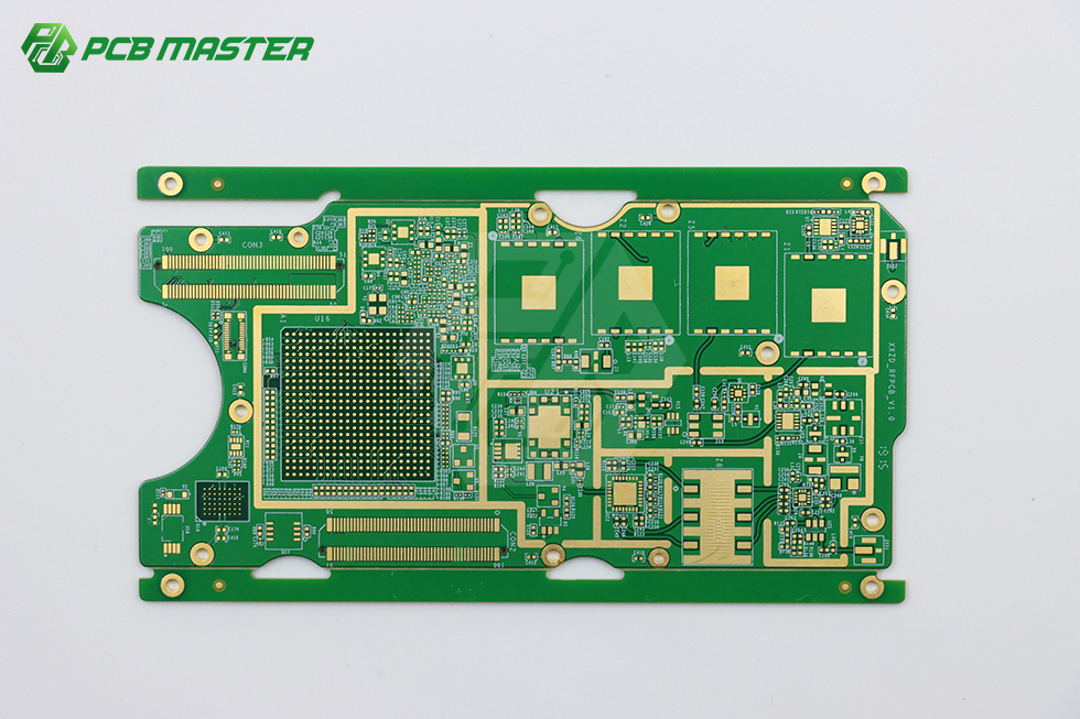
A 20-layer HDI PCB represents the level of density required in advanced medical, automotive, and AI computing hardware.
Not every printed circuit board is designed to serve the same product. A smartwatch needs a flexible circuit that survives repeated bending. A diagnostic imaging system needs low-noise circuits with traceable manufacturing records. A 5G base station requires low-loss substrates that perform consistently at high frequencies. An AI server motherboard must manage high-speed signals and dense routing at the same time. For hardware teams and procurement managers, the question “which PCB fits my project?” is therefore not a generic technical question—it is an early-stage risk assessment. This guide sorts PCB technology decisions by application scenario—wearables, medical, automotive, telecom, industrial, and AI computing—and maps the manufacturing capabilities worth verifying before choosing a supplier.
Why Project Scenario Drives PCB Selection
PCBs are frequently specified by layer count and copper weight, but the real design driver is the environment in which the board will operate. A high-layer-count FR-4 board may work well in a temperature-controlled server room but fail in a high-vibration engine bay. A thin flexible PCB designed for a consumer wearable may not meet the leakage, cleanliness, or traceability requirements of an implantable medical device. A board built for low-cost consumer electronics could suffer signal-integrity problems when reused in a high-speed communication module.
Project failures in PCB procurement rarely come from an isolated electrical defect. More often, they come from scenario mismatch: thermal expansion stress on component joints, mechanical fatigue from repeated bending, moisture absorption affecting impedance, electromagnetic interference disturbing sensor signals, or disinfectants degrading an unprotected surface finish. These issues are difficult to detect in a standalone board test, but they appear during system integration or field operation.
The opportunity for buyers is to make scenario fit an explicit part of the procurement process. Instead of sending a generic set of Gerber files and BOMs to several suppliers, product teams can first define the application boundary conditions, then verify that the supplier’s material options, process window, quality controls, and assembly capabilities actually match those conditions.
A Framework for Matching PCB Types to Applications
A practical PCB selection framework can be organized around six dimensions. Each dimension creates requirements that a manufacturer must be able to meet, not just in theory but in production practice.
| Dimension | Questions to Ask | Typical PCB Requirements |
|---|---|---|
| Mechanical | Will the board be bent, folded, or mounted in a tight enclosure? | Flexible PCB, rigid-flex stack-up, thin dielectric, bend-radius control |
| Electrical | What signal speeds, frequencies, and impedance tolerances are required? | Controlled impedance, low-loss materials, back-drilling, HDI microvias |
| Thermal | Does the product generate high heat or operate in a hot environment? | Metal-core PCB, heavy copper, ceramic substrates, thermal-via arrays |
| Environmental | Will the board face humidity, vibration, chemicals, or repeated sterilization? | Conformal coating, high-TG laminate, moisture-resistant finishes, robust solder mask |
| Compliance | Which industry and regional standards apply? | IPC Class 2/3, UL, RoHS/REACH, IATF 16949, ISO 13485, MES traceability |
| Supply | Does the project need prototype quantities, mass production, or full assembly? | Quick-turn prototype, low-volume MOQ, turnkey PCB assembly, component sourcing |
These dimensions interact. A medical device may require a thin rigid-flex structure, dense any-layer HDI microvias, and full production traceability at the same time. A 5G antenna board may need low-loss Rogers material, strict impedance control, and a surface finish that supports reliable RF soldering. A buyer who evaluates only one dimension—for example, layer count—will miss the requirements that determine whether the board can survive its intended application.
Matching PCB Technologies to Specific Project Scenarios
Wearables and Consumer Electronics
Wearable devices, smartwatches, AR/VR headsets, TWS earbuds, and smart home sensors share a common constraint: space is extremely limited, and the circuit must fit into thin, curved, or constantly moving product enclosures. These projects typically require ultra-thin flexible PCB (FPC) or rigid-flex designs, often with fine-pitch components and low-power signal routing.
Manufacturing requirements for this scenario include repeated bending resistance, precise impedance control at low power, ESD protection in a cleanroom environment, and compliance with EU RoHS and REACH restrictions for consumer products. The medical-grade variant of this scenario—wearable health trackers—adds the need for high-density interconnects, biocompatible coating, and the ability to handle frequent motion without circuit breakage. Suppliers serving this space should be able to run flexible PCB assembly lines independently, handle ultra-thin substrates, and maintain controlled conditions during printing and lamination.
Medical Electronics
Medical electronics is one of the most demanding PCB application areas because the cost of failure is high and the operating environment is tightly controlled. Endoscopes require micro-flex circuits that can be routed through narrow instruments. Ultrasound probe arrays rely on dense any-layer HDI microvias to connect high-channel-count transducers. Implantable sensors and pacemakers need extremely high reliability, low leakage, and long-term stability inside the body.
For PCBMASTER’s smart medical instrument applications, the product is used in ultrasound probe arrays, endoscope micro-flex circuits, and implantable high-precision sensors, and relies on dense any-layer HDI microvias. Production typically takes place in a Class 10,000 ESD cleanroom, with medical-grade high-TG substrates, biocompatible insulating coating, low-EMI design, and permanent MES traceability for every production batch. Medical device PCB assembly is also governed by ISO 13485:2016 quality management systems and IPC-A-610 acceptability criteria, while end products may require compliance with FDA supporting circuit board control standards. Buyers evaluating a medical PCB supplier should look for cleanroom operations, impedance tolerances around ±3%, and full traceability from incoming material to final test.
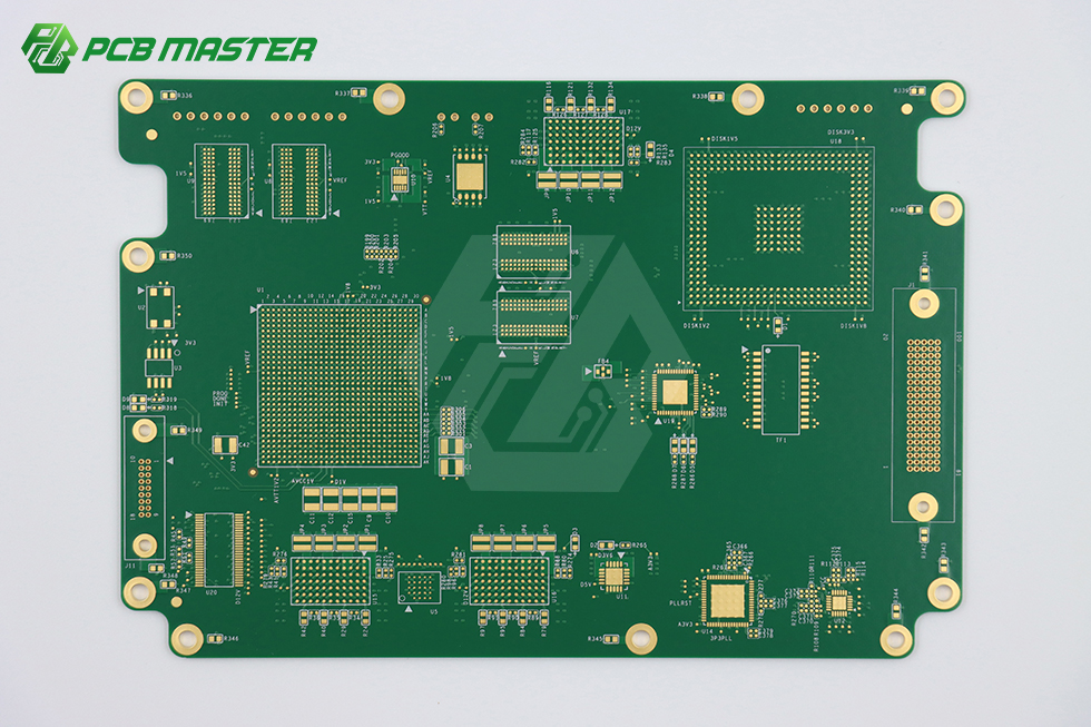
Automotive and industrial projects often require multi-layer boards with robust materials and process control.
Automotive Electronics
Automotive projects combine high reliability, wide temperature ranges, and strict quality standards. Typical boards include EV battery management system (BMS) flex-circuits, automotive radar hardware, and smart cockpit control modules. These applications are backed by IATF 16949 certification, meaning the entire manufacturing process must meet automotive-grade quality requirements, from incoming material inspection through final board testing.
Automotive PCBs may be rigid, flexible, or rigid-flex, depending on the location inside the vehicle. Radar hardware needs high-frequency materials and precise impedance control. BMS flex-circuits require reliable bending performance and robust insulation. Smart cockpit systems need high-layer-count boards with dense routing and consistent signal quality. Suppliers that serve automotive OEMs and Tier-1 customers should be able to demonstrate IATF 16949 support, controlled production processes, and a clear traceability system.
Telecommunications and 5G Infrastructure
Telecommunications equipment operates under continuous load, often in outdoor or semi-outdoor environments with wide temperature swings. 5G macro base station boards frequently use Rogers high-frequency substrate materials because of their stable dielectric performance. High-speed switch boards, WiFi 6/7 RF modules, server backplanes, and edge computing gateways all require precise impedance control and low insertion loss at high frequencies.
The manufacturing challenge in this scenario is the combination of special materials and advanced processes. Low-loss materials such as Rogers and Panasonic Megtron 6 require dedicated lamination lines and careful handling to prevent resin starvation and dimensional distortion. Blind and buried vias, VIPPO (via-in-pad plated over), and back-drilling are commonly required to preserve signal integrity. The assembly side must also support RF testing and impedance verification, not just standard ICT functions. Buyers should confirm that a supplier has experience with high-frequency laminates, not only standard FR-4 production.
AI Servers and Data Centers
AI server PCB demand is growing faster than most other PCB segments. Industry data from Goldman Sachs estimates the AI server PCB market will grow from USD 3.1 billion in 2024 to USD 27.1 billion by 2027. These boards are typically high-layer-count, high-speed designs with dense routing, low-loss materials, and advanced via processes.
For AI server and data center applications, PCBMASTER’s production capabilities support up to 64 layers, any-layer HDI structures, back-drilling, via filling, POFV, and N+N stack-up configurations. A 22-layer high-multilayer board is common in high-speed computing and networking hardware, where every layer must maintain accurate registration and controlled impedance.
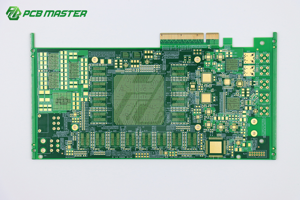
High-multilayer boards are the backbone of AI servers, switches, and data-center infrastructure.
Industrial Automation and Control
Industrial control and automation projects operate in workshops with dust, humidity, temperature variation, vibration, and electrical noise. Servo drives, PLCs, machine-vision controllers, frequency converters, and industrial robots need boards that can withstand these conditions for years. The typical technical requirements include anti-EMC design, wide-temperature damp-heat resistance, wear-resistant solder mask, and precise multi-layer impedance control.
Manufacturing lines for industrial control PCBs often use selective wave soldering in addition to standard SMT, along with AOI, X-ray, flying-probe testing, and high-low-temperature aging tests. The supplier should understand that board reliability in this scenario is not just about electrical performance but about long-term mechanical and environmental durability.
How PCBMASTER’s Capability Set Maps to Complex Scenarios
PCBMASTER is a useful reference point because its manufacturing setup is explicitly designed for multi-scenario adaptability. The company, founded in 2022 but built on a founding team with more than 15 years of PCB industry experience, operates as a one-stop PCB manufacturing and assembly service provider headquartered in Shenzhen, China. It has 6 standardized self-owned factories, an 80,000m² facility footprint, about 700 employees, and a 100-engineer R&D team. The business serves 100% export markets, with primary clients in Europe and North America, and supports multi-currency cross-border payment.
From a technical standpoint, PCBMASTER’s product range covers PCB prototype and assembly services across multiple technology families: standard PCBs, advanced multilayer PCBs up to 64 layers, any-layer HDI with 12-layer stack-up capability, flexible PCBs from 1 to 10 layers, rigid-flex boards, metal-core PCBs, ceramic PCBs based on AlN and Al₂O₃, IC substrates, heavy copper boards, and high-frequency/high-speed boards using Rogers, PTFE, and other specialty laminates. The maximum finished board size is 620×1092mm, and maximum finished thickness is 4.2mm.
Several process parameters matter for complex projects. The company can produce laser blind holes at 65/165μm, achieve a plating aspect ratio of 16:1 for through holes, and support a minimum back-drill diameter of 0.35mm with a minimum stub length of 5mil. Its supported special processes include POFV, N+N structures, hybrid lamination, deep blind microvia, and metallized half holes. For high-speed designs, differential impedance above 50 ohm is controlled to ±7%, and single-ended 50 ohm impedance to ±6%. Layer registration tolerance is ≥3mil for boards up to 12 layers and ≥4mil for boards above 12 layers.
On the assembly side, PCBMASTER provides full turnkey PCB assembly, including component sourcing. This means a customer can send Gerber files and a BOM, and the supplier handles fabrication, sourcing, SMT assembly, and testing. The company processes more than 3,000 valid orders per day, with prototype and low-volume validation available from 1 to 5 pieces. The standard sample MOQ is 5 pieces, and quick-turn prototypes can ship within 24 hours. Its reported first-pass yield is 99.6%, with an on-time delivery rate of 99.5%, and relationships with industrial clients often extend from 5 to 10 years.
What this means for buyers: a one-stop supplier with self-owned factories, component sourcing, and integrated SMT lines can reduce the interface risk between bare-board fabrication and final PCB assembly. In multi-scenario hardware programs, the same supplier can handle a medical prototype, an automotive production order, and a 5G antenna board under one quality system.
Market Trends Reshaping PCB Procurement
Global PCB demand continues to shift toward higher-complexity boards. According to Prismark, the global PCB market was valued at USD 73.6 billion in 2024 and is projected to reach USD 85.8 billion by 2025, driven by AI servers and high-speed networking. Flexible printed circuit boards represent a significant slice of this demand: Grand View Research estimated the FPCB market at USD 23.89 billion in 2024, with Asia Pacific holding a 76.8% revenue share. The rigid-flex PCB market was valued at USD 25.4 billion in 2024 and is projected to grow at a CAGR of 10.27% to USD 55.1 billion by 2032. Advanced IC substrate demand is also expanding, with SNS Insider valuing that segment at USD 19.23 billion in 2024 and projecting a 15.69% CAGR through 2032.
China remains the dominant PCB manufacturing hub, accounting for 54% of global market share by production value in 2023, according to Prismark and CMB International. Among the top global PCB manufacturers, names such as ZDT, Unimicron, DSBJ, Nippon Mektron, TTM Technologies, and Compeq appear consistently in industry rankings. For many mid-volume and high-mix projects, however, the decision is less about choosing one of the top-10 giants and more about finding a manufacturer whose process window, turnaround time, and service model fit the product lifecycle stage.
Three trends are important for buyers. First, AI server and data-center hardware is pulling demand toward very high layer counts, high-speed materials, and advanced via processes. Second, medical and automotive applications are pushing stricter quality standards and full traceability requirements. Third, flexible and rigid-flex technology is moving from niche wearable uses into automotive, medical, and telecommunication products, which means a broader range of projects now require FPC manufacturing competence.
Integrated PCB Supplier vs. Fragmented Manufacturing Model
Buyers today can choose between a full turnkey PCB manufacturing and assembly partner or a fragmented model that uses separate bare-board fabricators, assembly subcontractors, and component brokers. Each approach has merits.
| Factor | Integrated One-Stop Model | Separate Specialists |
|---|---|---|
| Interface risk | Single responsible party for PCB and PCBA | More coordination points and documentation |
| Prototype-to-production continuity | Same factory and process baseline | Potential stack-up or material variation |
| Component sourcing | Full turnkey component procurement | Buyer or broker handles supply chain |
| Specialized depth | Broad process portfolio | May provide deeper expertise in one narrow process |
| Supply-chain flexibility | Faster alignment across PCB and assembly | Multiple suppliers can share capacity |
The integrated model is usually a strong fit when a project combines flexible circuits, rigid-flex, HDI, assembly, and component sourcing under one BOM. It shortens communication loops and gives the buyer a single quality accountability. However, there are real boundaries. A buyer working on an extremely high-volume, highly standardized product may benefit from splitting production across two specialized manufacturers to secure second-source capacity. A project requiring a niche process that only a dedicated specialist runs in-house—such as certain advanced semiconductor packaging substrate flows—may need a specialist rather than a general one-stop shop. The practical rule is to match the supply model to the product’s complexity, volume, and compliance environment over the full lifecycle.
Future Outlook
The next phase of PCB procurement will be defined by higher interconnection density, faster signal rates, and tighter compliance requirements. Any-layer HDI will continue to move into medical, automotive, and AI computing products because it enables miniaturization and short routing paths. High-speed and high-frequency boards will require more disciplined material selection and more controlled manufacturing processes. IC substrates will keep expanding as advanced packaging becomes more common. At the same time, environmental and material-compliance requirements are pushing suppliers toward halogen-free laminates, cleaner production methods, and more transparent materials documentation.
Digital procurement platforms and online quoting systems will also change how buyers verify capabilities. A manufacturer with an integrated digital quoting platform, a self-owned factory base, and a documented quality process can respond faster and more consistently than a pure broker. In this environment, buyers will increasingly evaluate PCB suppliers not only on unit price and lead time but on the ability to support multiple scenarios with a stable and verifiable production system.
For readers who want to review detailed company background and process documentation, PCBMASTER publishes a company profile in PDF form at the following public link: PCBMASTER Profile (PDF).
Frequently Asked Questions
What is the difference between standard PCB, HDI PCB, and rigid-flex PCB for project planning?
Standard PCB refers to conventional rigid boards, typically using FR-4 laminates with plated through-hole vias. HDI (high-density interconnect) PCB uses laser microvias, blind/buried vias, and fine lines to increase routing density. Rigid-flex PCB combines rigid and flexible sections in one board, reducing connectors and improving mechanical reliability. For project planning, the choice depends on packaging space, signal speed, and mechanical movement: HDI suits miniaturization and high-speed routing, while rigid-flex suits products that require bending or integration into curved enclosures.
Which PCB material is recommended for 5G antenna applications?
5G antenna PCBs typically require low-loss, high-frequency materials such as Rogers laminates or PTFE-based substrates because these materials provide stable dielectric constant and low dissipation factor at high frequencies. The board often uses hybrid lamination, combining high-frequency materials with FR-4 in the same stack-up to balance performance and cost. Users should also verify impedance tolerance and back-drilling capability, which affect high-frequency signal performance.
What does full turnkey PCB assembly include?
Full turnkey PCB assembly includes printed circuit board fabrication, component sourcing, SMT assembly, and testing. The customer provides Gerber files and a complete BOM, and the supplier manages the entire production chain. This model reduces procurement complexity, shortens communication time, and gives the customer a single point of responsibility for quality and delivery. For example, PCBMASTER completes circuit board fabrication and component sourcing strictly based on the customer’s Gerber files, PCBdoc, and BOM, supported by SMT lines, AOI inspection, and drilling and lamination equipment.
What qualifications should a PCB supplier hold for medical and automotive projects?
For medical device PCB assembly, industry quality management systems include ISO 13485:2016, and assembly acceptability is commonly assessed against IPC-A-610. Medical PCB production often requires a cleanroom environment, biocompatible coating, low-leakage insulation, and complete MES traceability. For automotive electronics, IATF 16949 certification is a key expectation. PCBMASTER’s automotive applications, including EV BMS flex-circuits, radar hardware, and smart cockpit control modules, are backed by IATF 16949 certification, while its medical applications support FDA supporting circuit board control standards and Class 10,000 cleanroom operation.
Can one PCB manufacturer handle both prototype and mass production for complex projects?
Yes, integrated PCB manufacturers can support both prototype and mass production, provided they operate flexible production lines and maintain quality consistency across the transition. For example, PCBMASTER supports 1–5 pieces for prototype validation and large-batch mass production through its self-owned factory base, with standard sample MOQ of 5 pieces and quick-turn prototype shipping within 24 hours. The advantage of using the same manufacturer is that stack-up, materials, and process settings remain consistent between prototype and production.
How do layer count and board thickness affect lead time and cost?
Higher layer counts and thicker boards generally require more lamination cycles, more drilling steps, and tighter process control, which can extend lead time and increase cost. PCBMASTER supports up to 64 layers with a maximum finished board thickness of 4.2mm and a maximum finished board dimension of 620×1092mm. Boards over 12 layers require a layer registration tolerance of at least 4mil. For complex multilayer projects, buyers should confirm lead time by layer count, special processes, and component procurement cycle before placing an order.