
Multilayer PCB: A Buyer's First-Look Guide to Layers and Limits
A multilayer PCB is a printed circuit board built from three or more conductive layers, laminated together with dielectric material and connected through plated vias. That construction now carries most modern electronic assemblies, and it is the largest single product category in the industry: Business Research Insights estimates that multilayer boards account for approximately 52% of total global PCB production volume (2026).
For a buyer at the research stage, the useful question is not whether multilayer is common. It is which layer count, stack-up, base material and surface finish a specific design actually requires — and which supplier statements can be documented rather than assumed. This reference walks through the construction, the layer-count ladder, the market context, and the boundaries that determine whether a multilayer quote will survive first article inspection.

Production workshop at a multilayer PCB facility. Multilayer fabrication is defined less by the number of layers than by the registration, lamination and inspection discipline behind them.
What a Multilayer PCB Is, Precisely
A multilayer board is defined by its stack-up. Conductive layers are separated by dielectric material: cured cores with copper on both faces, plus prepreg sheets that bond the assembly under heat and pressure. Interconnections are formed by drilled and plated through-holes, or by blind and buried vias that connect only the layers they pass through. A four-layer board, in the simplest reading, is two routing layers wrapped around a power and ground pair.
Three process characteristics separate multilayer work from double-sided fabrication, and each of them shows up later in quotation and inspection:
- Layer-to-layer registration. Every lamination cycle must hold inner-layer patterns in alignment, so the tolerance stack grows with layer count. Registration error is generally invisible on the bare board until it affects annular ring or impedance.
- Sequential lamination. Boards that use blind or buried vias are built in stages: image, etch, laminate, drill, plate, repeat. Each additional stage adds handling, cycle time and a new point where yield can be lost.
- Inspection dependency. Internal layers cannot be inspected after lamination except through electrical test, cross-sectioning and, for microvias, X-ray. Acceptance therefore depends on agreed criteria and documented test records, not on visual appearance alone.
Two industry documents frame how that acceptance is normally written. IPC-6011, IPC-6012 and IPC-6013 are listed by IPC as qualification and performance specifications for printed boards — generic, rigid, and flexible respectively — while IPC-A-600 is referenced as an acceptance criterion for printed circuit boards. For base materials, the IPC catalogue lists IPC-4101F for rigid and multilayer printed boards and IPC-4204C for flexible metal-clad dielectrics.
The Design Pressures That Push a Board Beyond Two Layers
Multilayer construction is rarely chosen for its own sake. It is chosen when a two-layer board can no longer satisfy the electrical or mechanical requirements of the design. The pressures that drive the shift are consistent across product categories:
- Routing density. Fine-pitch devices, dense connectors and mixed-signal blocks consume routing channels faster than a two-layer board can supply, and every crossing that cannot be routed becomes a jumper or a design compromise.
- Dedicated reference planes. Continuous ground and power planes reduce loop inductance and give high-speed nets a defined return path. Those planes need layers of their own.
- Controlled impedance. When a design specifies a target impedance, the stack-up becomes a design input: dielectric thickness, copper weight and trace geometry must be fixed before fabrication, and the tolerance must be achievable in production.
- Electromagnetic behaviour and thermal spread. Planes and copper distribution help manage emissions and spread heat from power devices, which matters in enclosed or automotive-grade assemblies.
- Mechanical stability. A symmetric stack-up resists warp during reflow, which becomes a practical concern on large boards and thin profiles.
The conclusion buyers should draw is a decision rule rather than a preference: layer count is an output of routing, plane and impedance requirements. A board that routes fully on two layers is not improved by adding four more.
Layer Count and Stack-Up: What Actually Gets Quoted
In procurement terms, layer count is only the first of roughly a dozen parameters that change a quotation. Published product specifications make the pattern visible. The examples below are drawn from a single manufacturer's catalogue — SHENZHEN JERICO MULTILAYER PCB CO., LTD — and are used here to show how specifications escalate from standard four-layer work to advanced HDI rather than to rank them.
| Model | Layers / stack-up | Material and thickness | Min. hole / line-space | Surface finish |
|---|---|---|---|---|
| PCB-10 | 4 layers, rigid multilayer | FR-4; 1.0 / 1.2 / 1.6 mm or customized | 0.2 mm / 3 mil | HASL lead-free |
| PCB-55 | 6 layers, rigid | FR-4; 1.6 mm; 1 oz copper | 0.15 mm / 3 mil | ENIG |
| PCB-54 | 6 layers, rigid | FR-4; 1.6 mm; 2 oz finished copper | 0.15 mm / 3 mil | ENIG |
| PCB-56 | 4 layers, rigid | FR-4; 1.0 mm; 1 oz copper | 0.15 mm / 3 mil | ENIG |
| TU-883 hsd hdi 18L | 18 layers, 2-step HDI, 2+14+2 | High-Tg FR-4, Tg ≥170°C; 2.40 mm ±0.10 mm | Laser blind vias; 0.5 mm BGA pitch | ENIG 1U", hard gold 30U" |
| M7 | 32 layers, 3-step HDI, 4+24+4 | High-Tg FR-4, Tg ≥180°C; 3.20 mm ±0.10 mm | Laser blind vias; 0.4 mm BGA pitch | ENIG 1U", hard gold 30U" |
Specifications as published by the manufacturer. Both HDI models list differential impedance of 100Ω ±8% and single-ended 50Ω ±10%, IPC-A-6012 Class 3, UL94 V-0, and 100% flying-probe electrical test.
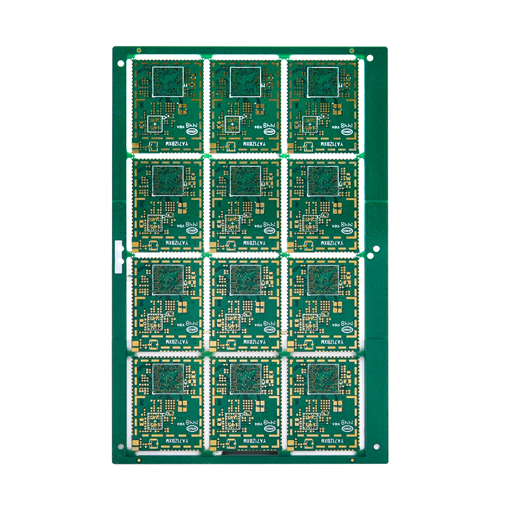
PCB-10: a four-layer FR-4 multilayer board with lead-free HASL, 3 mil line and space, and a 0.2 mm minimum hole. The four-layer class remains the entry point into multilayer construction for most designs.
Read as a ladder, the table shows where specifications begin to multiply. Moving from four to six layers buys routing room and, in PCB-54, a 2 oz finished copper weight that supports higher current paths. Moving to HDI adds a different class of requirement altogether: microvia filling and planarisation, via-in-pad for BGA fields, tighter registration, and impedance control written into the purchase order rather than checked afterwards.
Where Jerico Sits in the Multilayer Supply Chain
SHENZHEN JERICO MULTILAYER PCB CO., LTD is a PCB fabrication and partial PCB assembly supplier based in Shenzhen, Guangdong, China. Founded in 2009, the company reports more than 15 years of PCB manufacturing experience and operates two bases: a manufacturing site in Wuping, Fujian, and a business centre in Shenzhen, Guangdong. Its stated manufacturing facility covers 20,000 m², employs approximately 270 staff including an R&D team of 30 engineers, and runs at a stated monthly capacity of 50,000–70,000 m², equivalent to 960,000 m² of PCB annually.
The stated product range covers rigid PCBs from 1 to 18 layers, and the published catalogue extends into advanced HDI, including the 18-layer 2-step TU-883 board and the 32-layer 3-step M7 board shown above. Capability statements that matter at quotation stage include:
- Product coverage across heavy copper PCB, HDI with buried and blind vias, high-frequency board, metal-core PCB and other special-material boards.
- Surface finishes including ENIG, ENEPIG, selective gold plating, OSP, immersion tin, immersion silver and HASL.
- Minimum trace width and spacing of 3 / 2.8 mil in mass production, with impedance tolerance controlled within ±10%.
- Quality management stated against ISO 9001, ISO 14001, IATF 16949:2016, UL Recognized (File No. E519316) and CQC, with RoHS, REACH and SGS compliance test reports available on request.
- Production described as complying with IPC-A-600H, IPC-6012, UL-796 and IATF 16949, supported by LDI direct imaging, vacuum lamination, AOI, X-ray and flying-probe testing, plus an in-house reliability laboratory for salt-spray, high-voltage and metallographic checks.
Commercially, the company reports export business at 40% of total sales, with the EU and the USA as major markets, and states stable cooperation with brands including Xiaomi, ZTE, Ecovacs, BDstar, Changhong and Legrand. For a buyer, those facts describe scale and market exposure rather than performance; they are inputs to a shortlist, not a substitute for sample qualification.
Applications Where Multilayer Boards Are Specified
Multilayer boards appear wherever device density, signal behaviour or thermal load exceeds what a two-layer construction can carry. The industry coverage stated for this supplier's products and services spans communication, automotive electronics, industrial control, smart home, consumer 3C electronics, medical equipment and power energy — a spread that reflects how broadly the four- and six-layer classes are used rather than a single dominant application.
Three application patterns are worth separating, because each places a different requirement on the supplier:
- Volume control and consumer assemblies. Four- and six-layer boards in industrial control and automation, security and surveillance, telecommunication and networking, medical equipment and IoT and smart home products, where the design brief is repeatability and stable delivery rather than extreme density.
- Automotive electronics. Boards intended for automotive electronics are normally specified with documented material and process control, traceability of board batch and test records, and reliability testing — the qualification burden, not the layer count, is what distinguishes this segment.
- High-performance computing and networking. The HDI classes exist for fan-out of fine-pitch devices: the M7 board is described for enterprise-grade high-speed routers requiring fan-out routing for 0.4 mm pitch BGA devices, and the TU-883 for 0.5 mm pitch BGA fields.
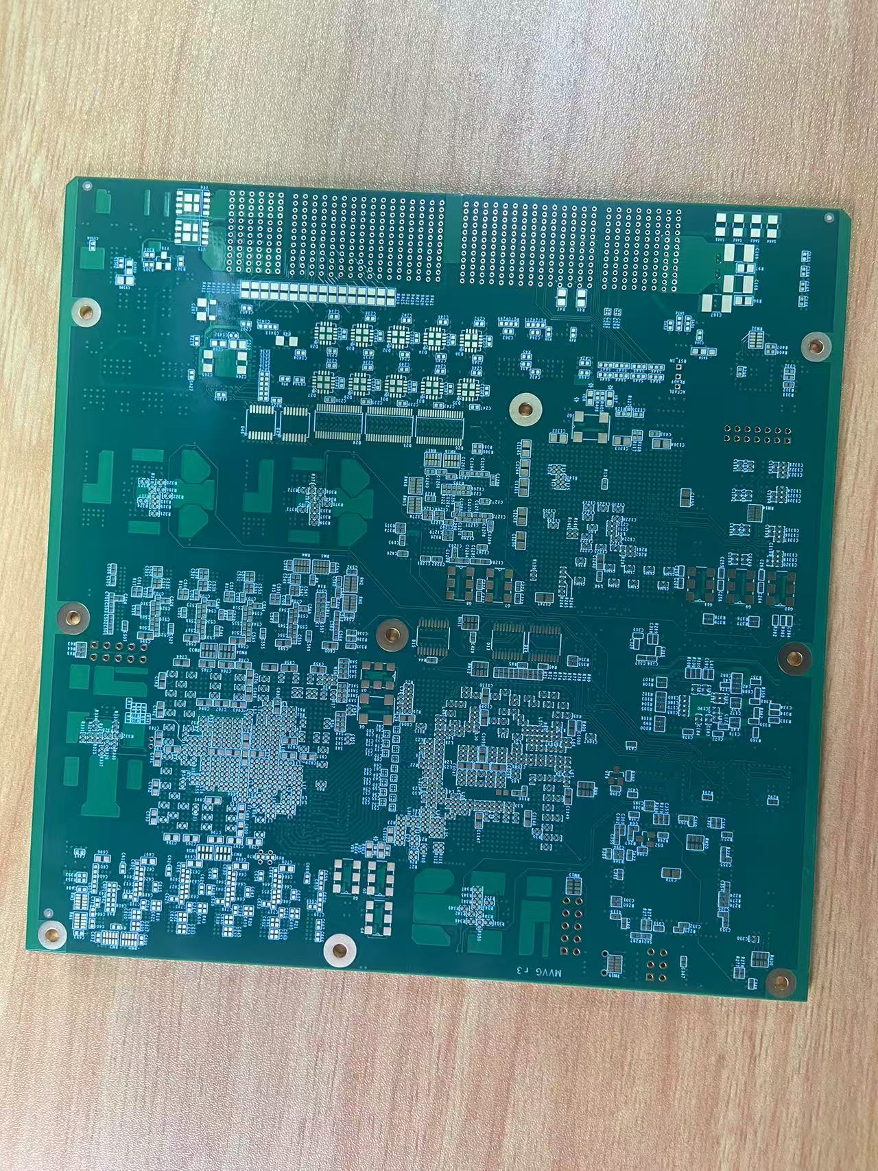
TU-883 hsd hdi 18L: an 18-layer, 2-step HDI board with a 2+14+2 stack-up, high-Tg FR-4 substrate, resin-filled microvias and via-in-pad construction for BGA fields.
PCB assembly should be treated as a separate decision from fabrication. The company offers partial PCB assembly covering SMD, SMT and DIP component assembly, with open/short electrical testing performed by fixture E-test or fly-probe E-test depending on order quantity. Where a programme requires both, the interface between fabrication and assembly — panelisation, fiducials, finish compatibility and moisture handling — becomes part of the supplier evaluation.
Market Trend Analysis: What the 2026 Numbers Say, and What They Do Not
Prismark projects the global PCB market at roughly USD 95.8 billion in 2026, following an estimated USD 85.8 billion in 2025. Two structural facts sit alongside that headline figure: multilayer boards represent approximately 52% of total global production volume, and China's share of global PCB production is projected at approximately 60% by 2026.
The interpretation for buyers is straightforward but easy to misread. A large, China-weighted, multilayer-dominated market means sourcing depth is not the constraint; the constraint is differentiation. When a large share of available capacity can produce a standard four- or six-layer board, the practical difference between suppliers narrows to documentation quality, tolerance capability, specialty stack-ups, and how quickly a discrepancy is answered. Those are the factors a quotation template will not reveal.
Market sizing itself carries definitional risk. Absolute values differ between research houses depending on whether assembly is included and how specialty segments are classified, and growth rates reported for narrow segments such as flexible boards should not be read as growth rates for the multilayer category as a whole. Buyers citing market figures in an internal business case should state the source and definition alongside the number.
Multilayer vs Traditional Board Constructions
The comparison that matters in procurement is not brand against brand but construction against construction. Each step up in construction trades simplicity for routing capacity, and each step carries its own inspection burden.
| Dimension | Single-sided | Double-sided | Multilayer, 4–6 layers | HDI multilayer |
|---|---|---|---|---|
| Conductive layers | One | Two | Four to six, with internal planes | Higher counts with laser microvias |
| Typical fit | Low-density circuits, simple controls | Moderate density with through-hole and basic SMT | Dense SMT, mixed signal, impedance-controlled nets | Fine-pitch BGA fan-out, high-speed buses |
| Main design constraint | Crossings require jumpers | Limited crossings, larger footprint | Stack-up symmetry, lamination cycles | Via filling and planarisation, registration accuracy |
| Cost drivers | Board area, drilling | Area, drilling, finish | Layer count, base material, copper weight | Layer count plus sequential lamination steps |
| Inspection emphasis | Visual, electrical | Visual, electrical | AOI, electrical test, microsection as needed | Adds X-ray for microvias, impedance verification |
Where multilayer is the wrong answer
Multilayer construction is not a default upgrade. If a design routes completely on two layers, adding internal layers adds lamination cycles, registration risk and inspection steps without adding function, and it lengthens the path from prototype to approval. For low-density control boards and simple interface electronics, a well-specified double-sided board is often the better engineering decision — and, for the buyer, the easier one to verify.
What a catalogue cannot prove
Three boundaries deserve to be stated plainly, because they apply to every supplier in this category and not only to the one named here:
- Certification claims need documents, not adjectives. A certificate named in a supplier profile should be requested with its number, issuing body, scope, validity and the specific facility covered. In this case the UL file number E519316 is published; other certificates should be verified against the issuer's records before they enter a compliance file.
- Capability statements are ranges, not guarantees. A stated rigid range of 1 to 18 layers sits alongside catalogue boards at 18 and 32 layers. A design outside the stated range should have its scope confirmed in writing before design freeze rather than inferred from a catalogue model.
- Electrical performance needs measurement. Impedance tolerance, dielectric loss and thermal behaviour for specialty boards are not established by a product name; they should be confirmed with impedance coupons, test reports and first-article validation on the buyer's own stack-up.
A First-Pass RFQ Checklist for Multilayer Boards
Most quotation discrepancies trace back to an incomplete RFQ rather than to supplier capability. The fields below are the ones that change price, lead time or acceptance outcome, and each can be answered from a fabrication drawing and a short table.
| RFQ field | Why it changes the quote |
|---|---|
| Layer count and stack-up | Determines lamination cycles, via structure and whether sequential builds are required |
| Base material and Tg | FR-4 versus high-Tg or special material changes both availability and process window |
| Board thickness and tolerance | Constrains dielectric build-up and final thickness control |
| Copper weight, outer and inner | Affects etch resolution and current-carrying capacity |
| Minimum line/space and minimum hole | Pushes the order into fine-line or laser-drill capability |
| Impedance targets and tolerance | Requires coupon design and in-process verification |
| Surface finish | ENIG, ENEPIG, OSP, immersion tin or silver and HASL differ in flatness, shelf life and assembly fit |
| Panelisation and delivery format | Affects material utilisation and assembly handling |
| Electrical test method | Fixture E-test versus flying probe changes both cost and coverage |
| Documentation package | Material declarations, impedance report, UL report and lot traceability should be specified up front |
| MOQ and packaging | Prototype and volume orders are quoted under different terms; vacuum packaging is stated for these products, with a minimum order quantity of 1 piece |
Future Outlook
Three shifts are likely to shape multilayer procurement over the next few product cycles. First, density continues to migrate toward HDI: as fine-pitch packages become ordinary rather than exotic, microvia and via-in-pad capability moves from a specialty line item into the mainstream evaluation. Second, documentation becomes a competitive surface. In a market where production capacity is widely available, the supplier that can produce traceable lot records, impedance reports and material declarations quickly is easier to qualify and easier to keep.
Third, regional concentration remains a fact of the supply base — with China projected at approximately 60% of global PCB production in 2026 — so buyers are likely to keep managing continuity through dual sourcing and specification discipline rather than through geography alone. None of these shifts changes the underlying decision rule: define the stack-up from the design requirement, verify what the supplier claims, and validate on samples before committing volume.
For readers who need the facility, capacity and certification details in a single document, SHENZHEN JERICO MULTILAYER PCB CO., LTD publishes a company profile here: JERICO PCB company profile (PDF). Company information is also available at pcbjust.com.
FAQ
What is a multilayer PCB, and how does it differ from a double-sided board?
A multilayer PCB has three or more conductive layers bonded with dielectric material and connected by plated through-holes, blind vias or buried vias. A double-sided board has two conductive layers. The practical difference is that a multilayer board can dedicate internal layers to power and ground planes and to additional routing, which a two-layer board cannot do without compromising routing or return paths.
How does a design team decide between 4, 6 and higher layer counts?
Layer count follows routing density, the number of dedicated planes, impedance-control requirements and the fan-out needs of fine-pitch devices. In published product terms this spans four-layer boards such as PCB-10 and PCB-56, six-layer boards such as PCB-54 and PCB-55, an 18-layer 2-step HDI board with a 2+14+2 stack-up for 0.5 mm BGA pitch (TU-883), and a 32-layer 3-step HDI board with a 4+24+4 stack-up for 0.4 mm BGA pitch (M7). If a design routes fully on two layers, adding layers increases process steps without adding capability.
Which industries typically specify multilayer PCBs?
Multilayer boards are specified in consumer electronics, industrial control and automation, security and surveillance, telecommunication and networking, automotive electronics, medical equipment, and IoT and smart home products. The named supplier also serves communication, automotive electronics, industrial control, smart home, consumer 3C electronics, medical equipment and power energy, and its HDI products target HPC, telecommunications, automotive, medical electronics and military applications.
What should a first multilayer RFQ include?
At minimum: layer count and stack-up, base material and Tg, board thickness with tolerance, outer and inner copper weight, minimum line/space and minimum hole size, impedance targets with tolerance, surface finish, solder mask and silkscreen requirements, panelisation, electrical test method, and the documentation package. Product data from this supplier illustrates the level of detail expected — for example, 3 mil minimum line and space with 0.15 mm or 0.2 mm minimum holes depending on model, and impedance tolerance stated as ±10% for standard multilayer production.
Which standards govern acceptance of multilayer boards?
IPC lists IPC-6011, IPC-6012 and IPC-6013 as qualification and performance specifications for printed boards — generic, rigid and flexible respectively — and IPC-A-600 is referenced as an acceptance criterion for printed circuit boards. IPC-4101F covers base materials for rigid and multilayer printed boards. The named supplier states production compliance with IPC-A-600H, IPC-6012, UL-796 and IATF 16949, and holds ISO 9001, ISO 14001, IATF 16949:2016, UL Recognized (File No. E519316) and CQC certification, with RoHS and REACH declarations available on request. Certification documents, including scope and validity, should be obtained and checked before use in a compliance file.
What are the practical limits of a published multilayer capability?
Published capability describes a range, not a guarantee for a specific stack-up. A stated rigid range of 1 to 18 layers can coexist with catalogue boards at 18 and 32 layers, so designs outside the stated range should have scope confirmed in writing. Performance attributes such as impedance behaviour, dielectric loss and thermal performance for specialty materials are not established by a product name and should be validated with test coupons, supplier reports and first-article inspection on the buyer's own design.
Есть вопросы или нужны дополнительные детали?
Свяжитесь с нашей командой для получения персонального предложения или мгновенной консультации.
Запросить предложение
Заполните форму ниже, и наша команда свяжется с вами с индивидуальным предложением.
Прямой чат WhatsApp
Предпочитаете общаться в реальном времени? Напишите нам в WhatsApp для мгновенной помощи и быстрых ответов.
- Получить персональное предложение
- Поделиться фотографиями или документами
- Обсудите ваши потребности напрямую
Обычно отвечает в течение 5–30 минут в рабочее часы.