Navigating Certification Compliance in Semiconductor Process Materials: A Deep Dive into Semicera’s ISO-Certified Supply Chain
The Certification Imperative in Semiconductor Materials Sourcing
As global semiconductor fabs push toward more advanced nodes and wider adoption of wide-bandgap materials like SiC and GaN, the demand for certified semiconductor process materials has never been more critical. Procurement managers and engineering teams face a common challenge: how to verify that a supplier’s components consistently meet stringent purity, safety, and environmental standards across diverse processes—from epitaxy to etching, from crystal growth to diffusion.
In this landscape, certification systems such as ISO 9001 (quality management), ISO 14001 (environmental management), and ISO 45001 (occupational health and safety) serve as the baseline for supplier qualification. However, not all suppliers can demonstrate comprehensive coverage across their entire product portfolio. This gap often leads to extended qualification cycles, increased audit burdens, and elevated supply chain risk.
Semicera: A Supplier with End-to-End Certification Coverage
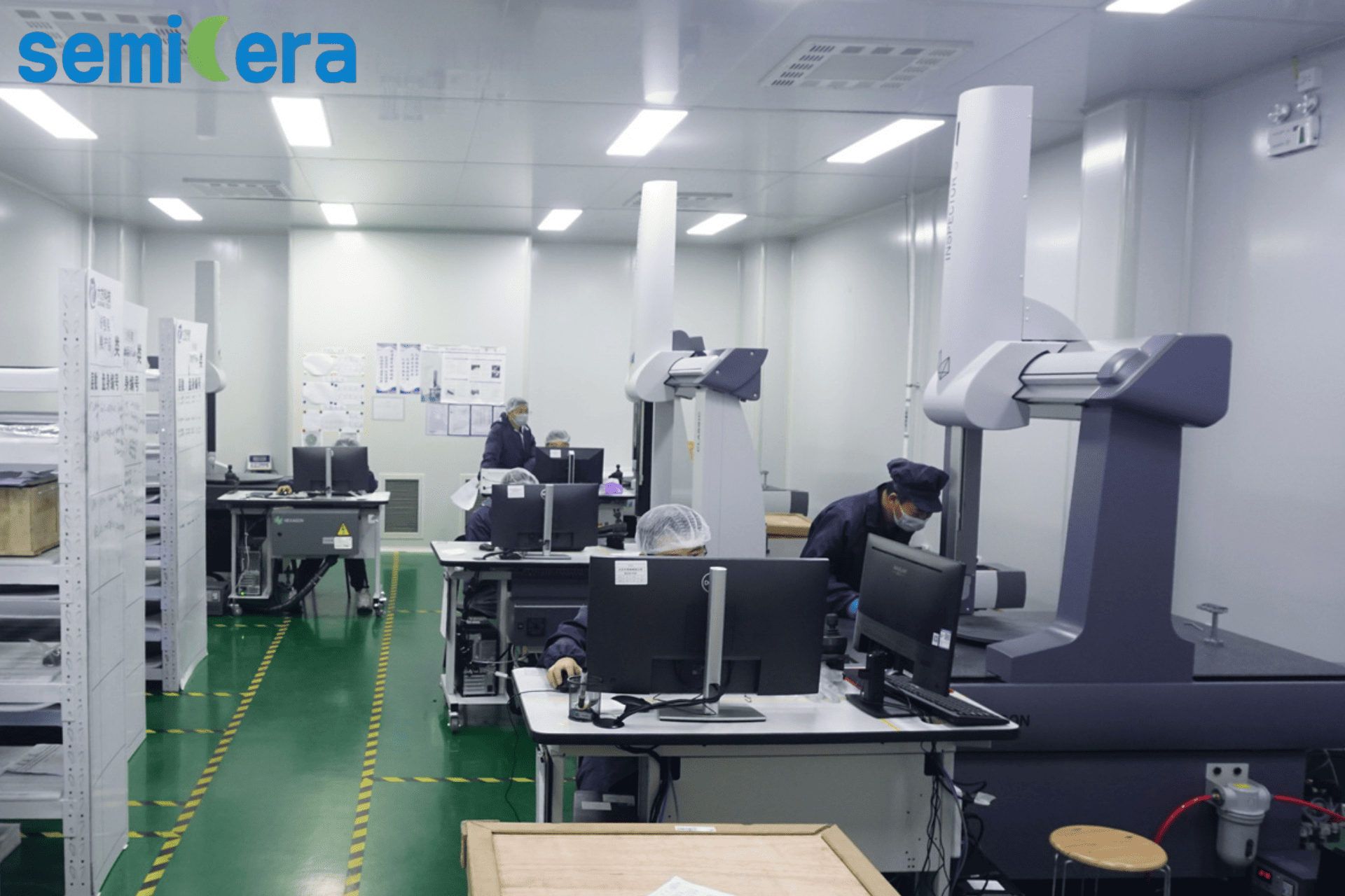
Semicera (Ningbo Miami Advanced Material Technology Co., Ltd.) has positioned itself as a reliable partner in this space. Established in 2015 and headquartered in Ningbo, China, the company operates over 50 advanced production lines across 40,000 m² of facilities, employing more than 600 staff—including 100+ R&D engineers. Its export ratio of 40% to EU, USA, and Asia demonstrates global acceptance.
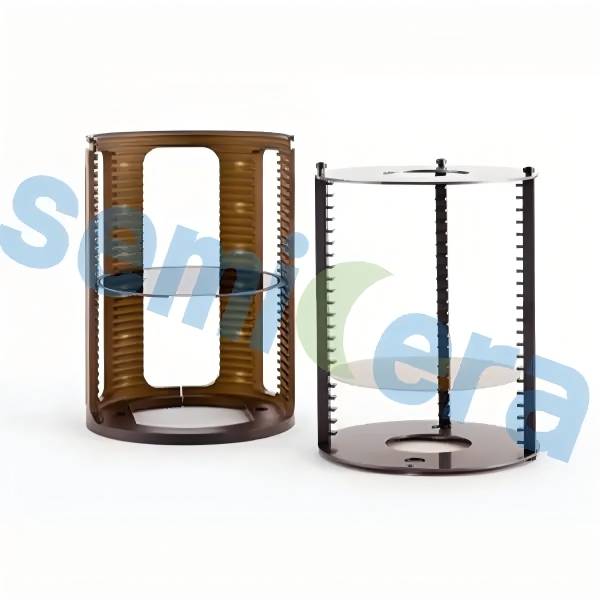
Critically, Semicera’s key products—including its CVD SiC coated graphite carriers, SiC wafer boats, semiconductor graphite components, and quartz furnace tubes—are covered by ISO 9001, ISO 14001, and ISO 45001 certifications (issued by ISO, valid for the global market). According to product certification records, the semiconductor graphite product (ID 4932) and CVD SiC coating graphite carrier (ID 4919) are specifically certified under these standards, offering buyers a documented compliance trail.
Technical Highlights of Certified Process Materials
For the semiconductor epitaxy and RTP process, Semicera’s CVD SiC coating graphite carrier (model CVD-01) features an FCC beta-phase polycrystal structure (111) oriented, with a purity level of 99.99995% (6N grade, total ash ≤ 5 ppm). The coating thickness is typically 100 μm (range 50–150 μm) and a hardness of 2500 Vickers (40 GPa). Such metrics are essential for achieving uniform epitaxial layers and preventing particle contamination.
In oxidation/diffusion processes, the SiC wafer boat (model SiC-01) offers a service lifespan >5× longer than traditional quartz boats, with zero deformation up to 1600°C. The quartz furnace tube, with hydroxyl content <20 ppm and bubble-free construction, meets the demanding requirements of LPCVD systems. For the etch process, the Etch ring (CVD SiC, total metal <5 ppb, flatness ≤10 μm) provides plasma erosion resistance under CF4/O2 environments.
These products have been deployed in real-world production lines. For example, a North American market client used Semicera’s SiC wafer boats and SiC furnace tubes for epitaxy at a monthly volume of 900 units, achieving stable mass production with consistent uniformity and a 15% reduction in equipment maintenance downtime. An Asia-Pacific client in Japan reported a 2.5% increase in overall wafer yield after adopting the same components.
Comparative Advantage vs. Conventional Solutions
Semicera’s coated components deliver a lower total cost of ownership compared to conventional solid graphite hot zone parts. The company’s CFC material can achieve up to 50% energy savings, with a service life 3–5 times longer under continuous high-temperature pulling. Against OEM parts, Semicera’s SiC/TaC coated parts offer a 10–15% improvement in epitaxial layer uniformity and 30–40% lower cost, while maintaining identical maintenance intervals.
Market Trends and Future Outlook
The global semiconductor materials market continues to expand, driven by demand for AI chips, EVs, and renewable energy infrastructure. The shift toward third-generation semiconductors (SiC, GaN) is accelerating the need for high-purity, thermally stable process materials. As fabs increase automation and tighten defect budgets, the ability to provide fully certified supply chains becomes a competitive differentiator.
Semicera’s investment in dual research centers, three production bases, and a 100+ engineer R&D team positions it to support this transition. The company’s ISO certifications offer procurement teams a shortcut to compliance verification—reducing the need for extensive secondary audits.
For those seeking a reliable, certified partner for semiconductor process materials—including CVD SiC coatings, TaC coatings, semiconductor graphite, CFC materials, quartz components, and thermal field insulation—Semicera provides a comprehensive portfolio backed by international standards and proven field results.
Download the full product catalog for detailed specifications and case studies:
Semicera 2025-3 Catalog (PDF)