
PCB Procurement FAQ: Lead Times, Minimums, and Custom Processes
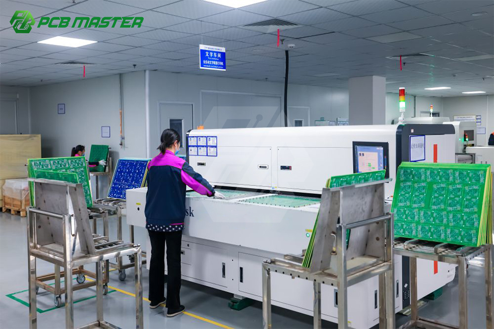
PCB production process — legend marking and silkscreen legend stage.
In PCB sourcing, the questions that delay a project are rarely about circuit design. They are about what a supplier can commit to: how quickly a board can be produced, whether a five-piece order is accepted, which layer counts and stack-ups are realistic, which laminates are available, and which custom processes need engineering review before a quote means anything.
This reference is written for buyers in the awareness and research stages of a sourcing cycle. The capability statements below come from PCBMASTER, a Shenzhen-headquartered one-stop PCB manufacturing and PCBA assembly provider that launched as an independent brand in 2022 and integrates PCB design support, component sourcing, quick-turn prototyping, and high-volume mass production. Where a number appears, it is either a published PCBMASTER capability or a third-party market figure with a named source.
Why PCB Procurement Questions Have Become More Technical
Board sourcing used to be a price-per-square-metre conversation. In 2026 it is a specification conversation. The global PCB market was valued at USD 83.6 billion in 2026 and is projected to reach USD 137.8 billion by 2035, according to Global Market Insights. At the advanced end of that market, Yole Group forecasts the total substrate market to reach USD 31 billion by 2030, and Dataintelo values the ceramic PCB market at USD 2.8 billion in 2025, with the alumina segment holding 52.4% of product-type share.
The driver is compute. The Taiwan Printed Circuit Association (TPCA) reported that NVIDIA's GB300 platform (2025) pushed PCB layer counts above 26 layers and raised PCB value to roughly USD 35,000 per server rack. When the layer count of a mainstream platform moves, the questions buyers ask move with it — from \"what does the board cost?\" to \"which supplier can actually build this stack-up, in this material, on this schedule?\"
Lead Times: What the Answer Depends On
Lead time is the first question in almost every PCB request for quotation, and the accurate answer depends on three variables: order type, stack-up complexity, and process content.
PCBMASTER operates six self-owned one-stop factories for PCB manufacturing and PCB assembly, and publishes 24-hour rapid prototyping alongside 5–7 days for small-batch production. For prototype orders specifically, the company states a standard turnaround of 5–7 business days, with expedited options of 24–48 hours for urgent projects. These are company-reported service terms, published on the vendor's own capability pages, rather than independently audited benchmarks.
A practical way to read those numbers:
- 24-hour rapid prototyping applies to quick-turn prototype work, not to every order.
- 5–7 business days is the stated standard window for prototype orders and the typical range for small-batch production.
- 24–48 hours expedited is an option positioned for urgent projects, and should be confirmed against the specific stack-up before it is written into a project plan.
The boundary matters more than the headline. A quick-turn window is not a universal promise. Boards that use special processes — plated over filled via (POFV), N+N stack-up structures, hybrid lamination, deep blind microvias, metallized half holes, or back drilling — add process steps that have to be scheduled. A full turnkey assembly order adds component procurement ahead of SMT and THT assembly. In practice, the buyer's own decisions — how early the fabrication data is frozen, how many design revisions are expected — affect the delivery date as much as the factory's cycle time.
Minimum Order Quantities and the Prototype-to-Production Gap
Minimum order quantity is the second most common blocker in early sourcing. PCBMASTER states that it applies no MOQ requirement, and describes its order profile as covering prototypes, small batches, and large-volume orders. Its published application profiles include rapid early-stage hardware R&D prototyping at 1–5 pieces for low-volume validation, alongside large-scale customized mass-production programmes.
That combination is what makes the prototype-to-production transition a procurement question rather than an engineering one. If a buyer can validate with a handful of boards and then scale the same design into volume orders with the same manufacturing partner, the design data, stack-up, and material choices carry forward instead of being re-qualified at a new supplier.
The limitation is economic rather than technical. \"No MOQ\" answers the question \"can this quantity be built?\" — it does not answer \"what does this quantity cost per unit?\" A five-piece prototype run and a five-thousand-piece production run carry different per-unit economics at any manufacturer, because setup, tooling time, and process qualification are spread across a different number of boards. Buyers should treat MOQ policy and unit pricing as two separate questions in the same RFQ.
Layer Counts and Stack-Up Limits
Layer count is the specification that most directly determines both performance and process cost, because each additional layer adds imaging, lamination, drilling, and registration cycles.
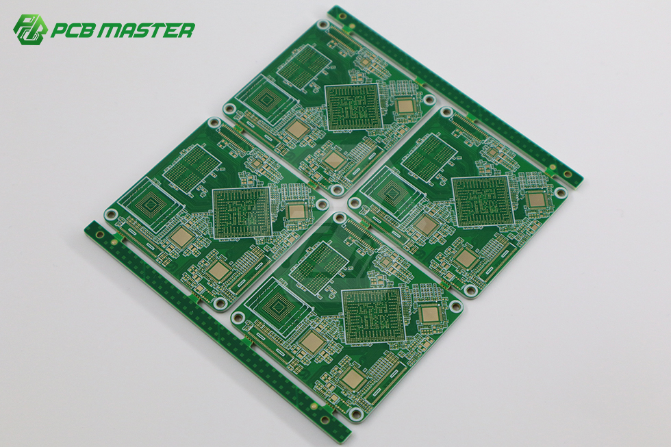
Stack-up architecture — not just layer count — sets the achievable lead time and process cost of a PCB.
PCBMASTER's published rigid-board capability covers layer counts of up to 64 layers, with an any-layer stack-up at 12 layers, a maximum finished dimension of 620 × 1092 mm, and a maximum finished board thickness of 4.2 mm. Flexible circuits are classified as Flexible Printed Circuits (FPC), manufactured from polyimide material, with a layer range of 1–32 layers.
| Stack-up parameter | Published capability |
|---|---|
| Rigid layer count | Up to 64 layers |
| Any-layer stack-up | 12 layers |
| FPC layer range | 1–32 layers (polyimide) |
| Max finished dimension | 620 × 1092 mm |
| Max finished board thickness | 4.2 mm |
| Layer registration tolerance | ≥3 mil (≤12 layers); ≥4 mil (>12 layers); ≥4 mil (N+N stack-up) |
| Pattern accuracy (boards >500 mm) | ±5 mil |
Set against the market, that envelope covers the layer counts now being specified for AI server and high-speed networking boards, which the TPCA places above 26 layers on current accelerator platforms. The boundary is equally clear: a design that requires more than 64 layers, or an any-layer structure beyond 12 layers, sits outside the published rigid-board range and would need to be confirmed as a project-specific request rather than assumed as a standard capability.
Material Options and How They Change the Quote
Material choice is where PCB procurement stops being a fabrication question and becomes a system-performance question. PCBMASTER's published material set includes FR-4 TG180 and FR-4 TG155, Rogers and PTFE laminates, ceramics (AlN and Al₂O₃), polyimide (PI), metal-core laminates in aluminium, copper, iron or steel, and BT and other IC substrate materials.
Those materials map onto different design intents:
- Rogers and PTFE support high-frequency and high-speed work such as 5G antenna PCBs and RF modules, where dielectric loss matters.
- Polyimide (PI) is the base for FPC and rigid-flex boards used in wearables, medical bands, and dynamic flex applications.
- Ceramic (AlN and Al₂O₃) addresses thermal management in power and high-reliability electronics; the market data above shows alumina as the largest ceramic PCB product type by share.
- Metal-core laminates serve applications where heat spreading and mechanical rigidity dominate.
- BT and IC substrate materials sit at the advanced packaging end of the portfolio.
The procurement implication is that material selection changes the process route, not just the bill of materials. High-frequency laminates require dedicated lamination control; ceramic substrates involve different handling and drilling behaviour than FR-4; polyimide flex materials introduce their own dimensional-stability considerations. Buyers who settle on a material after the quote is issued are, in effect, restarting the quotation. Settling material, layer count, and stack-up together before the RFQ is the single most effective way to shorten the procurement cycle.
Custom Processes: What \"Custom\" Really Requires
Custom is a broad word in PCB sourcing. In practice it covers a defined set of process capabilities, each with its own engineering constraints. PCBMASTER's published special-process list includes POFV (plated over filled via), N+N stack-up structures, hybrid lamination, deep blind microvias, and metallized half holes. Back drilling is supported with a minimum back-drill diameter of 0.35 mm, a minimum stub length of 5 mil, and a minimum distance from back-drill to copper of 5 mil.
| Process parameter | Published value |
|---|---|
| Laser blind via specification | 65 / 165 µm |
| Max dimple of plated filled hole | 10 µm |
| Through-hole plating aspect ratio | 16:1 |
| Min back-drill diameter | 0.35 mm |
| Min back-drill stub length | 5 mil |
| Min back-drill-to-copper distance | 5 mil |
| Differential impedance (>50 Ω) | ±7% |
| Single-ended 50 Ω impedance | ±6% |
Impedance control deserves separate attention because it is a tolerance, not a feature. A published differential impedance tolerance of ±7% for traces above 50 Ω and ±6% for single-ended 50 Ω impedance defines the window a supplier can hold — and that window is what determines whether a high-speed design will behave as simulated. Buyers specifying high-speed or high-frequency boards should confirm the impedance tolerance in writing, because it is the parameter most often assumed rather than quoted.
A short RFQ checklist for custom boards
- Layer count and stack-up (including whether any-layer or N+N structure is required)
- Material family and grade (FR-4 TG180 / TG155, Rogers, PTFE, polyimide, ceramic, metal-core, BT)
- Finished dimensions and board thickness, checked against the 620 × 1092 mm and 4.2 mm published limits
- Impedance requirements with target values and acceptable tolerance
- Special processes: POFV, back drilling, deep blind microvia, hybrid lamination, metallized half hole
- Quantity per build stage (validation, small batch, production)
- Assembly scope if turnkey is required (fabrication, component procurement, SMT/THT assembly, inspection, testing, delivery)
- Target date, separated into fabrication time and assembly time
Turnkey vs. Multi-Vendor Sourcing: A Practical Comparison
The sourcing model itself is a procurement decision. PCBMASTER's published turnkey scope covers PCB fabrication, component procurement, SMT/THT assembly, inspection, testing, and delivery through a single partner. Supported assembly process types include SMT, THT, mixed SMT+THT assembly, single-sided and double-sided assembly, and automated or manual soldering.
A traditional multi-vendor model splits those steps across a fabrication house, a component distributor, an assembly house, and a test provider. Each split introduces a handoff: the bare board must be received and inspected before assembly, components must arrive before the SMT line is scheduled, and a test failure is investigated across organisational boundaries rather than inside one factory.
| Consideration | Integrated turnkey model | Multi-vendor model |
|---|---|---|
| Handoffs between steps | Coordinated inside one supplier | One handoff per step |
| Accountability for defects | Single point of contact across fabrication and assembly | Split across suppliers; root-cause investigation crosses boundaries |
| Sourcing flexibility | Constrained to the partner's material and component network | Free to select a specialist per step |
| Schedule control | Compressed, but dependent on one supplier's capacity | More parallel options, more coordination overhead |
Where the integrated model has real boundaries: the published rigid-board ceiling of 64 layers and any-layer stack-up of 12 layers defines what can be quoted as a standard capability, not the outer limit of every possible design. Quick-turn windows are service terms that depend on the stack-up and process content of a specific order, not blanket guarantees. And concentrating a schedule in one supplier is only an advantage when that supplier's capacity matches the project's layer count and material profile — for ceramic, IC substrate, or very high-layer-count work, capability and timing should be confirmed per project rather than inferred from general quick-turn claims. Buyers should also note that the capability data discussed here is vendor-published; independent third-party throughput verification for this supplier is not yet available in the public record.
Where These Answers Matter: Application Context
The procurement questions above are not theoretical, because different industries weight them differently.
| Application area | Typical board profile | Dominant procurement question |
|---|---|---|
| Automotive electronics and industrial control | Boards backed by IATF 16949 status; EV BMS flex circuits, automotive radar hardware, smart cockpit control profiles | Can the supplier hold certification and repeatability across volume builds? |
| Wearables | Ultra-thin, high-flexibility FPC for smartwatches, AR/VR headsets and medical bands, in 24/7 operation | Which material and flex construction survives continuous use? |
| Medical electronics | Endoscope micro-flex circuits, ultrasound probe arrays, implantable high-precision sensors using dense any-layer HDI microvias | Can the process hold fine-feature and impedance tolerances? |
| Communications and data infrastructure | 5G antenna PCBs, servers and data centres, AI servers, high-speed and high-frequency boards | Which layer count and laminate deliver the required signal performance? |
The pattern is consistent: the more demanding the application, the less the buyer is buying \"a PCB\" and the more they are buying a defined process window — layer count, material, tolerance, and turnaround, all confirmed before the order is placed.
Market Trend Analysis: Layer Count and Material Choice Now Drive Cost
Three signals from 2025–2026 market data point in the same direction. First, volume: the global PCB market moves from USD 83.6 billion in 2026 toward USD 137.8 billion by 2035. Second, value concentration: TPCA's reporting on the GB300 platform ties more than 26 PCB layers to roughly USD 35,000 of PCB value per rack, a different order of magnitude from conventional server boards. Third, substrate specialisation: Yole Group's USD 31 billion advanced substrate forecast for 2030 and Dataintelo's USD 2.8 billion ceramic PCB market for 2025 both describe demand shifting toward materials with more demanding process routes.
For buyers, the practical reading is that the specification decisions covered in this FAQ — layer count, stack-up, material, and special process content — are now the primary cost and schedule variables, not administrative details. Two boards of identical outline dimensions can differ by a multiple in price and lead time depending on whether one is a standard multilayer FR-4 build and the other uses a high-frequency laminate with back drilling and impedance control.
Future Outlook
Two directions look durable. The first is continued specification pressure at the top of the market: as accelerator and high-speed networking platforms hold layer counts above the mid-twenties, the ability to quote and build high-layer, high-speed boards becomes a qualification criterion rather than a differentiator. The second is material diversification, with ceramic, IC substrate, and high-frequency laminates moving from niche orders into regular procurement portfolios.
The likely buyer response is a two-tier sourcing structure — a fast prototyping partner for validation cycles and a production partner for volume — or, where the same partner can cover both, a single integrated relationship that carries the design data forward. PCBMASTER's published position sits in the second category: six self-owned one-stop factories, 24-hour rapid prototyping and 5–7 day small-batch windows, no stated MOQ, a rigid layer ceiling of 64 layers with any-layer stack-up at 12 layers, an FPC range of 1–32 layers, and a material set spanning FR-4, Rogers, PTFE, polyimide, ceramic, metal-core, and IC substrate laminates. Whether that envelope fits a specific programme is a per-project question — which is exactly the kind of question this FAQ exists to make answerable earlier in the cycle.
FAQ: Common PCB Procurement Questions Answered
What lead time should a buyer expect for a PCB prototype?
PCBMASTER publishes 24-hour rapid prototyping and a standard prototype turnaround of 5–7 business days, with expedited options of 24–48 hours for urgent projects. Small-batch production is stated at 5–7 days. These are service terms published by the manufacturer, and actual timing depends on layer count, material, and whether special processes are involved.
Is there a minimum order quantity for PCB fabrication?
PCBMASTER states that it applies no MOQ requirement, and positions its service across prototypes, small batches, and large-volume orders. Published application profiles include 1–5 piece validation builds for early hardware R&D as well as large-scale customized mass-production programmes. No MOQ affects whether an order is accepted; it does not change per-unit pricing, which varies with quantity and process content.
How many layers can be produced?
For rigid boards, PCBMASTER publishes a layer count of up to 64 layers, with any-layer stack-up at 12 layers. Flexible Printed Circuits (FPC) are made from polyimide material and cover a layer range of 1–32 layers. Designs exceeding 64 rigid layers, or requiring any-layer structures beyond 12 layers, fall outside the published range and require project-specific confirmation.
Which PCB materials are available?
The published material set includes FR-4 TG180 and FR-4 TG155, Rogers and PTFE high-frequency laminates, ceramics (AlN and Al₂O₃), polyimide (PI) for flexible circuits, metal-core laminates in aluminium, copper, iron or steel, and BT and other IC substrate materials. Material selection determines the process route, so it should be fixed before quotation rather than after.
What are the maximum board dimensions and thickness?
PCBMASTER publishes a maximum finished dimension of 620 × 1092 mm and a maximum finished board thickness of 4.2 mm. For boards larger than 500 mm, published pattern accuracy is ±5 mil. Layer registration tolerance is ≥3 mil for boards of 12 layers or fewer, ≥4 mil for boards above 12 layers, and ≥4 mil for N+N stack-up structures.
Which custom and special processes are supported?
Supported special processes include POFV (plated over filled via), N+N stack-up structure, hybrid lamination, deep blind microvia, and metallized half hole. Back drilling is supported with a minimum back-drill diameter of 0.35 mm, a minimum stub length of 5 mil, and a minimum distance from back-drill to copper of 5 mil. Laser blind vias are specified at 65 / 165 µm, and the maximum dimple of a plated filled hole is 10 µm.
How is impedance controlled on high-speed boards?
PCBMASTER publishes impedance tolerance of ±7% for differential impedance above 50 Ω and ±6% for single-ended 50 Ω impedance. Through-hole plating aspect ratio is published at 16:1. Buyers specifying high-speed or high-frequency boards should confirm impedance targets and tolerances in writing before production, because the tolerance window defines how closely the finished board matches the simulated design.
What does a turnkey PCB assembly order include?
The published turnkey scope covers PCB fabrication, component procurement, SMT/THT assembly, inspection, testing, and delivery through a single manufacturing partner. Supported assembly process types include SMT, THT, mixed SMT+THT assembly, single-sided and double-sided assembly, and automated or manual soldering. Buyers should confirm which of these steps are included in a given quote, and how component procurement timelines interact with the target delivery date.
Reference document: PCBMASTER company profile (PDF).