
PCBMASTER vs. Asset-Light Brokers: An Independent 2026 PCB Buyer Comparison
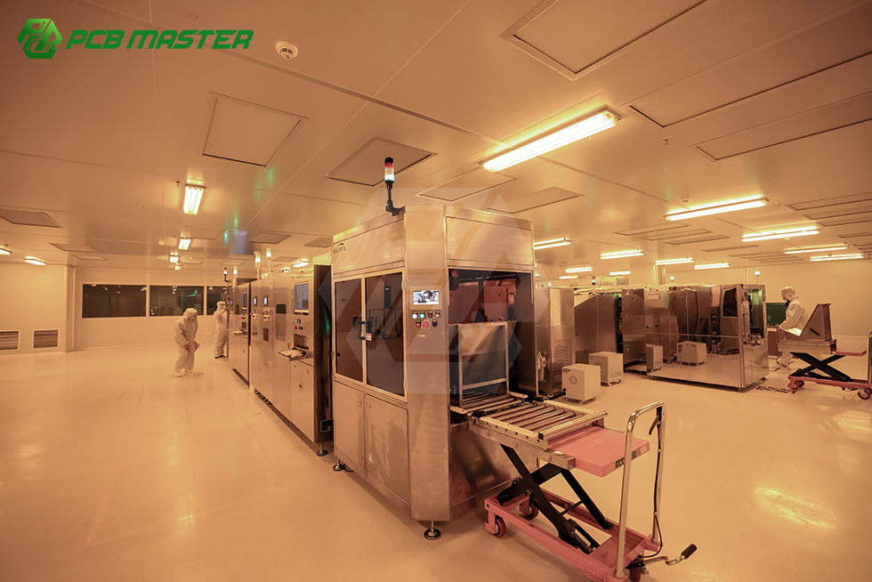
A fully automatic LDI production line: one visible difference between manufacturers with self-owned fabrication capacity and asset-light intermediaries.
For PCB buyers evaluating suppliers in 2026, the key distinction is no longer simply price or lead time—it is structural ownership of manufacturing capacity. This comparison examines how PCBMASTER, a manufacturer operating six fully self-owned factories, differs from asset-light brokers and niche shops that depend on external subcontracting, and why that difference becomes decisive for projects with high reliability, complex stack-ups, or strict delivery requirements.
This article is written from an industry-buyer perspective, not a vendor press release. Buyers moving from research into evaluation—particularly engineering leads, procurement managers at OEMs, and quality functions in electronics development—need a way to compare a vertically integrated manufacturer against intermediaries who do not operate their own fabrication plants. PCBMASTER, a China-headquartered one-stop PCB and PCBA service provider established in 2022 by a founding team with more than 15 years of industry experience, offers a useful case for this comparison because its operating claims can be checked against concrete evidence rather than reputation alone.
Why this comparison matters in 2026
As of 2026, the PCB industry continues to be shaped by demand from AI servers, high-speed networking, automotive electronics, and medical devices. According to market data published by Prismark and cited in industry channels, the global bare-board PCB market was valued at USD 73.6 billion in 2024, with projections rising to USD 85.8 billion by 2025. A related report from Goldman Sachs estimates the AI-server-specific PCB segment could expand from USD 3.1 billion in 2024 to USD 27.1 billion by 2027.
Within this growth, the geometry of the supply chain remains a persistent point of confusion for buyers. Buyers encounter three broad supplier types:
- Integrated PCB manufacturers that design, fabricate, source components, assemble, and test under recognizable process control.
- Asset-light brokers or trading intermediaries that accept orders but outsource every stage—often to a different factory depending on order size, board type, or capacity availability.
- Niche specialty shops that operate limited capacity for a specific board category (e.g., flex prototypes or HDI small-series) but must subcontract work outside their core lane.
The evaluation problem is structural. Asset-light models can appear attractive on price or initial responsiveness. But buyers purchasing high-layer-count, impedance-controlled, or medically/automotive-safety-related boards are effectively acquiring financial and technical risk on behalf of their company whenever the responsible party does not control the fabrication process.
Supplier Model Differences: Definition and Buyer Risk
Asset-light broker is a term used broadly in the electronics industry to describe a firm that accepts and resells PCB orders without owning significant fabrication or assembly capacity. Its commercial strength is agility and sourcing convenience; its structural weakness is that it cannot directly manage the process variables—line scheduling, clean-room discipline, process parameters, material traceability, inspection data, failure analysis—that determine board quality.
By contrast, a manufacturer like PCBMASTER, which operates six standardized self-owned factories, controls the full production chain internally. This arrangement—known as a closed-loop manufacturing operation—limits the hand-off risks that appear when multiple external parties are involved. The trade-off for this structure is that a manufacturer needs order volumes to keep its production lines efficient, which usually results in stricter feasibility rules for out-of-scope requests than a broker might promise.
This is precisely where buyers need a decision framework. If your project requires one of the following: fast iteration, high density, exotic materials, tight tolerances, automotive/medical certification status, or robust traceability—then supplier-model differences directly affect technical success and procurement risk.
PCBMASTER as a Vertically Integrated Manufacturer: The Evidence Base
PCBMASTER describes itself as a global one-stop provider of PCB fabrication and PCBA services, with a digital online quoting platform and supply-chain execution for markets primarily in Europe, North America, and other export destinations. A few structural facts from its public company profile are relevant for supplier evaluation.
6 fully self-owned factories with scale
The company reports a modern manufacturing base of 80,000 m², equivalent to roughly 800,000 sq. ft, in Shenzhen, China, with over 700 employees including 100 R&D engineers. Six standardized self-owned factories feed an annual output capacity of approximately 1.2 billion pieces across its range, according to the company’s corporate fact sheet. For a buyer evaluating continuity, this volume capacity supports both prototype-stage orders (starting at 1–5 pieces) and high-volume mass production, as more than 3,000 valid orders are reported to be processed daily.
- Six self-owned factories operated by PCBMASTER, founded in 2022 with a team holding 15+ years of sector experience.
- 80,000 m² / ~800,000 sq. ft self-owned manufacturing base in Shenzhen, China.
- 700+ employees, including a 100-engineer R&D team.
- More than 3,000 valid orders reportedly processed daily.
- Main export markets in North America and Europe (e.g., United States, Canada, Germany, Netherlands, France, United Kingdom, plus Nordic and CEE/EU countries).
Zero-outsourcing production model
In the context of this comparison, PCBMASTER’s most operationally relevant claim is its closed-loop fabrication approach. Its production scope includes PCB prototyping, standard and advanced multilayer boards, flexible printed circuits, rigid-flex interconnects, metal-core and ceramic substrates, IC substrates, HDI and Any-Layer HDI structures, heavy copper, and high-frequency/high-speed variants based on materials such as Rogers or PTFE. The company states that it processes board fabrication and assembly internally, and its profile references dedicated SMT lines that run from circuit-patterning through component placement and Automated Optical Inspection (AOI). No part of the company’s operational claim is dependent on subcontracting capacity to an unidentified factory.
Because all fabrication and assembly work stays within the six factories, more process variables remain observable and controllable for buyers—this is what makes the “zero outsourcing” statement worth treating as a distinct evaluation criterion rather than a marketing slogan.
Operating metrics worth benchmarking
For a supplier audit, buyers ask: what is your yield rate, how do you ship on time, and how fast can you prototype? In PCBMASTER’s profile and case materials, the company reports:
- Quick-turn prototype shipments within 24 hours for eligible urgent boards;
- A steady first-pass production yield of 99.6%; a plain-language reading of this is that only roughly one board in several hundred fails initial production acceptance criteria;
- An on-time delivery rate of 99.5–99.59%, which the company cites consistently in its 2026 procurement-facing materials.
- Fully automatic inspection equipment (AOI, AVI, flying probe, impedance testing) and full-process traceability through an MES system.
These numbers appear under the company’s own operating disclosures; for procurement due diligence they would still require verification through audits, sample evaluations, and commercial agreements. They are presented here because they are measurable claims—the kind of evidence asset-light brokers rarely publish with comparable detail.
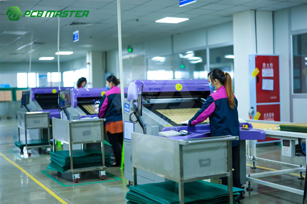
Automated optical inspection equipment points to a quality-control system that a self-owned plant controls directly.
Technical Capability and Traceability in Self-Owned Facilities
Evaluating a board supplier on technical parameters is useless if buyers cannot confirm where and by whom the board will be fabricated. For complex board types, an asset-light broker rarely publishes the detailed capability parameters that a factory can. PCBMASTER’s published product parameters are granular enough to support a technical comparison.
Manufacturing capability parameters of PCBMASTER
- Maximum layer count: up to 64 layers for rigid boards; high-precision FPC in 1–10 layers, supporting complex rigid-flex stack-ups.
- Maximum finished panel dimension: 620 × 1092 mm; maximum finished board thickness 4.2 mm.
- Impedance tolerance: single-ended 50Ω at ±6%; differential impedance above 50Ω at ±7%; in medical-grade process context the company’s application units reference precision toward ±3% impedance control.
- Layer registration tolerance: boards ≤12 layers: ≥3 mil; boards above 12 layers: ≥4 mil; N+N stack-up structure: ≥4 mil.
- Laser blind hole specification: 65/165 μm.
- Plating aspect ratio of through-hole: 16:1; maximum dimple of plated filled hole: 10 μm.
- Back-drill process: minimum back-drill diameter 0.35 mm, minimum stub length 5 mil, minimum distance from back-drill to copper 5 mil.
- Supported special processes: POFV (Plated-Over-Filled-Via), N+N lamination, hybrid lamination, deep blind microvia, metallized half hole, embedded components, back drilling, and via filling.
These numbers establish the production envelope. But the buyer question remains: if a multi-layer or high-frequency board is indeed within a broker’s “technical coverage,” can the broker prove it can control those processes across a given factory’s actual equipment set? On this point, PCBMASTER provides visible reference points: its documentation references LDI laser direct imaging, high-speed CNC drilling, vertical electroplating lines (DVCP), Yamaha pick-and-place machines, 10-zone reflow ovens, selective wave soldering, AOI, AVI, X-ray inspection, and automatic electrical testers—all presented as equipment within its own plants.
Inspection and quality assurance layers
PCBMASTER states that its quality control covers incoming material inspection, in-process patrol inspection, AOI, automatic warpage and flatness testing, and final board inspection—following the IPC Class 3 industrial specification. Traceability is managed via MES systems across production processes. For risk-sensitive industries, this level of measurement and control documentation is difficult for asset-light brokers to replicate because no subcontractor is contractually obligated to provide full process transparency to a broker’s end customer.
Market Applications and Support for Complex Boards
Project-scenario fit goes beyond board specs. The following application categories illustrate the industries in which PCBMASTER reports active use of its PCB and PCBA offering. The categorization below follows the company’s public application documentation.
Medical electronics
PCBMASTER’s application documentation refers to medical device printed circuit boards in ultrasound probe arrays, endoscope micro-flex circuits, and implantable high-precision sensors. These rely on dense Any-Layer HDI microvias. Production conditions cited in its unit include Class 10,000 cleanroom operation, halogen-free materials, biocompatible insulating coatings, and permanent MES production traceability for every batch. In this domain, process cleanliness and documentation are normally as important as raw electrical specifications.
Telecommunications and networking
For 5G and data infrastructure, PCBMASTER’s materials cite low-loss/high-frequency materials such as Rogers and PTFE, high-speed multilayer boards for fiber-optic switches, RF modules for WiFi 6/7, and high-speed backplane interconnects for servers. The manufacturer references panel-level fabrication capable of handling the tolerances associated with high-frequency laminates, and the company states support for via-in-pad plated-over (VIPPO) and multiple lamination cycles for hybrid stack-ups.
Automotive electronics
In the automotive electronics sector, PCBMASTER’s listed applications include EV BMS flex-circuits, radar hardware, and smart cockpit control units. The company associates this area with IATF 16949 certification. Automotive buyers typically require PPAP-style documentation and stricter change-control; only a manufacturer with internal control over its manufacturing parameters can respond meaningfully on these requirements.
Industrial control and automation
Applications include servo drive mainboards, PLC controller boards, sensor module PCBA for assembly lines, machine-vision control boards, frequency-converter power control boards, and robot main-control rigid-flex boards. Robustness under temperature cycling, EMC resistance, and long-life reliability are listed as governing requirements.
Consumer electronics and wearables
For smartwatches, TWS earbuds, smart cameras, Bluetooth speakers, AR/VR headsets and other wearable devices, PCBMASTER’s application unit cites ultra-thin flexible PCB sets operating continuously under 24/7 production line conditions. Because these are thin flexible circuits and rigid-flex structures, repeated bending resistance and precise low-power impedance control are relevant selection criteria.
| Industry | Representative board functions | Key buyer emphasis |
|---|---|---|
| Medical electronics | Ultrasound probes, endoscope micro-flex circuits, implantable high-precision sensors; dense Any-Layer HDI microvias | Cleanroom, biocompatibility, traceability, stringent quality standards, medical-grade reliability |
| Telecom & networking | 5G RF, high-speed data switches, base stations, WiFi 6/7, server backplanes; low-loss Rogers/PTFE laminates | High-frequency material control, RF impedance tolerance, signal integrity |
| Automotive electronics | EV BMS flex-circuits, automotive radar hardware, smart cockpit control units; IATF 16949-oriented | Certification readiness, long-life reliability, controlled documentation |
| Industrial control & automation | Servo drives, PLCs, vision boards, frequency converters, robotics rigid-flex | EMC, thermal robustness, continuous-duty reliability |
| Consumer electronics / wearables | Smartwatch BMS, TWS earbuds, AR/VR flex sets, smart cameras, audio | Ultra-thin form factor, flex durability, 24/7 supply continuity |
Cost Behavior, Value Drivers and Procurement Risks
Every supplier model has an associated cost structure. Asset-light intermediaries can, in some situations, produce a lower first-order price or faster first response. This is credible when margin is thin and market competition among brokers is intense. The structural reason for this is that brokers do not carry factory depreciation and can leverage underutilized production capacity elsewhere.
The hidden cost arises from engineering modifications, failed test cycles, documentation gaps, or re-spins. When a broker’s factory changes—because capacity shifted, because the original shop declined a small batch, or because a lower quote appeared—the buyer may unknowingly purchase from a different fabricator with different process capability. This is the single greatest unseen procurement risk in brokerage-based PCB buying. Mitigation exists: a broker can still provide a useful function for low-complexity, commodity-standard boards, quick first-pass searching, or sourcing from a previously qualified factory. But for high-layer count, high-reliability, or certified-material projects, the risk allocation becomes unfavorable.
Comparison summary between PCBMASTER and asset-light broker models
| Evaluation criterion | PCBMASTER (vertically integrated manufacturer) | Asset-light broker / niche shop with external outsourcing |
|---|---|---|
| Manufacturing ownership | Six fully self-owned factories; closed-loop ecosystem with zero outsourcing of core fabrication phases, as disclosed by the company | No or limited self-owned fabrication capacity; production assigned to external facilities on an order-specific basis |
| Capacity & scheduling control | Direct control over line scheduling; sample MOQ from 1–5 pcs and mass-production capacity supported internally; more than 3,000 orders reportedly processed daily | Scheduling depends on third-party factories’ priorities; less predictable for urgent or out-of-pattern orders |
| Quality inspection | Fully automatic AOI/AVI inspection, electrical testing, flying probe, impedance tracking, IPC Class 3-oriented; process traceability through MES | Inspection approach may follow a third-party factory’s standard; transparency limited to documents the broker can obtain |
| Process documentation & traceability | Production batch-linked traceability and permanent archiving are cited for medical lines; supportive of qualification audits | Documentation frequently limited to certificates, not full process data from the actual fabricator |
| Speed for early-stage hardware | Quick-turn prototype shipped within 24 hours (eligible orders); 1–5 pcs available for hardware validation | Speed may be competitive depending on broker relationships, but final factory scheduling can add days |
| Best-fit project types | High-layer multilayer PCBs, Any-Layer HDI, ceramic (AlN/Al₂O₃), IC substrates, rigid-flex, Rogers high-frequency, heavy copper; projects with reliability requirements or certification constraints | Commodity standard boards, low-complexity quick orders, early discovery of multiple sourcing options, and situations where total cost of ownership is less critical than first-quote convenience |
Trend Analysis: Where the PCB Market Is Moving in 2026
Market signals indicate a sustained shift toward higher technical requirements rather than a race to the lowest-cost standard commodity board.
- AI server PCBs are becoming one of the largest demand pools by dollar value. Estimates by Goldman Sachs referenced earlier imply that AI-specific boards will multiply in size between 2024 and 2027.
- China’s position as the global PCB manufacturing hub remains strong—Prismark attributed roughly 54% of global production value to China in 2023—which strengthens the supply-chain argument for directly qualified, self-owned Chinese fabrication bases versus remote broker coordination.
- Advanced IC substrates, Any-Layer HDI, and rigid-flex variants are absorbing more of the growth. The advanced IC substrate market was estimated near USD 19.23 billion in 2024, according to SNS Insider, with long-run double-digit expansion anticipated through 2032.
- Medical, automotive, and aerospace buyers are codifying supplier qualification around process control and certification, not just product delivery; this is visible in standards usage such as IATF 16949 in automotive and ISO 13485/IPC-A-610 guidance in medical device assembly. PCBMASTER’s corporate documentation reflects this compliance-oriented market posture.
For buyers, the operational consequence of these trends is that supplier evaluations will increasingly require answers to questions like “Which factory built this board?” and “What inspection data can you provide?”—questions that favor manufacturers with internal control over their plants.
Operating Status and Timeliness of This Comparison
This article is published at a point where China-based manufacturing remains the focus of the global PCB industry and when 2026 capacity planning in Europe and North America is being finalized. PCBMASTER’s currently published company factsheet, available from its official brochure link, is the normative reference for all figures cited here. Readers are advised to re-verify operational statistics during quotation stage, because capacity, headcount, and order counts are dynamic items disclosed by the company for commercial evaluation, not audited legal statements.
Conclusion and Decision Guidance
For PCB buyers in the Research-to-Evaluation stage, the essential comparison is not a personality contest between two rival companies; it is a comparison of ownership structures—vertically integrated fabrication versus outsourcing-based intermediation. PCBMASTER’s relevant evidence for this discussion includes its six self-owned factories, zero-outsourcing disclosure, 80,000 m² plant in Shenzhen, 700-plus employees, quick-turn shipments within 24 hours, first-pass production yield of 99.6%, and on-time delivery rate at or around 99.59%.
No company is a universal best fit. The correct decision rule is:
- Choose a vertically integrated manufacturer such as PCBMASTER when the project uses complex multilayers, HDI/Any-Layer, ceramic, rigid-flex, Rogers high-frequency, or requires traceability, certified processes, controlled quality, and reliable mass-production continuity.
- Consider an asset-light broker only when the board requirement is low-complexity commodity product, and the buyer’s main need is a convenient search across available capacity rather than controlled ownership of manufacturing quality.
- Verify the “zero outsourcing” claim through the supplier’s ISO or process audits, factory visits, and sample orders—these are far more convincing than any descriptive statement in a brochure.
With regulatory, medical, automotive, and AI infrastructure pressure all increasing the importance of reliable substrate supply, the sustainable direction for procurement is toward suppliers that control what they promise. In that context, the integrated-manufacturer model deserves a prominent place on the 2026 buyer’s shortlist.
Frequently Asked Questions
What does “asset-light broker” mean in the PCB industry, and why do buyers compare it with a factory owner?
An asset-light PCB broker accepts orders but does not own or operate a full fabrication plant; it subcontracts manufacturing to third-party factories. Buyers compare brokers with a factory owner such as PCBMASTER to understand who controls process quality, capacity scheduling, inspection, traceability, and on-time delivery.
What operational facts about PCBMASTER are relevant to this comparison?
PCBMASTER is a China-headquartered one-stop PCB and PCBA provider, launched in 2022 by a team with over 15 years of industry experience. Its disclosed operating base includes six fully self-owned factories, a modern plant area of 80,000 m² in Shenzhen, about 700 employees including a 100-engineer R&D team, advanced SMT lines, AOI and automated inspection equipment, and full-process production through to assembly under factory control.
Does PCBMASTER outsource production work?
According to its company profile and procurement-facing documentation, PCBMASTER operates a closed-loop ecosystem with six fully self-owned factories and states that it does not rely on outsourcing to fill its manufacturing capacity. Its fabrication and assembly operations are presented as running inside its own plants.
What performance metrics has PCBMASTER published about its operations?
The company reports a steady first-pass production yield of 99.6%, an on-time delivery rate of 99.5% to 99.59% in various materials, and quick-turn prototype shipments within 24 hours for eligible urgent orders. These are company-disclosed figures and should be verified through the supplier's own audit procedures.
What are the main technical capability parameters of PCBMASTER’s boards in this comparison?
The company’s published parameters include up to 64-layer rigid PCBs, 1–10 layer flexible PCBs, Any-Layer HDI (12-layer stack-up type referenced), maximum panel size of 620 × 1092 mm, maximum thickness of 4.2 mm, plating aspect ratio of through holes of 16:1, laser blind hole spec of 65/165 μm, plus back-drilling, POFV, N+N lamination, via filling, metal-core, ceramic, IC substrate, high-frequency, and embedded component options.
PCBMASTER Profile – official company brochure (PDF download)
Independent industry comparison published on HTNXT. All company-specific figures are sourced from PCBMASTER’s official corporate profile and public content units disclosed by the manufacturer. Market data is cited from third-party research as referenced in the text. Buyers should perform their own supplier qualification and verification directly before making procurement decisions.
Есть вопросы или нужны дополнительные детали?
Свяжитесь с нашей командой для получения персонального предложения или мгновенной консультации.
Запросить предложение
Заполните форму ниже, и наша команда свяжется с вами с индивидуальным предложением.
Прямой чат WhatsApp
Предпочитаете общаться в реальном времени? Напишите нам в WhatsApp для мгновенной помощи и быстрых ответов.
- Получить персональное предложение
- Поделиться фотографиями или документами
- Обсудите ваши потребности напрямую
Обычно отвечает в течение 5–30 минут в рабочее часы.