
PCBMASTER: Full Turnkey PCB Assembly for High-Reliability Projects
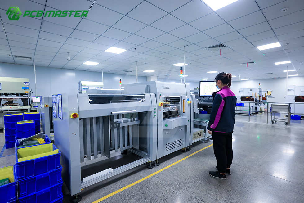
The global printed circuit board (PCB) market was valued at USD 73.6 billion in 2024 and is projected to reach USD 85.8 billion by 2025, driven by AI servers and high-speed networking. As demand surges for complex, high‑reliability boards, engineering and procurement teams face a persistent challenge: how to source prototype quantities and volume production without sacrificing quality, lead time, or control over the supply chain. Many OEMs still rely on separate vendors for PCB fabrication and assembly, introducing interface risk, extended cycle times, and inconsistent quality management. PCBMASTER, a global one‑stop provider headquartered in China, delivers integrated PCB manufacturing and turnkey assembly (PCBA) designed to bridge this gap — from quick‑turn prototypes to mass production.
Problem & Opportunity
Traditional procurement models often split PCB bare‑board manufacturing and component assembly across multiple suppliers. This fragmentation can lead to higher administrative overhead, increased potential for miscommunication on BOM and Gerber files, and prolonged qualification cycles. For projects requiring high‑layer‑count boards (up to 64 layers) or specialized materials — such as Rogers, PTFE, ceramic substrates (AlN, Al₂O₃), polyimide, or metal‑core — the lack of a single accountable partner forces engineers to become de‑facto project managers. The market also shows strong growth in sub‑segments: the AI server PCB segment alone is expected to surge from USD 3.1 billion in 2024 to USD 27.1 billion by 2027, while the advanced IC substrate market was valued at USD 19.23 billion in 2024 with a projected CAGR of 15.69% through 2032. These trends amplify the need for manufacturing partners who can handle both complexity and volume under one roof.
Brand Solution: Integrated Turnkey PCBA from Prototype to Volume
PCBMASTER is a premier, global one‑stop provider of Printed Circuit Board (PCB) manufacturing and assembly (PCBA) services. The company offers OEM contract manufacturing, component sourcing, and technical services worldwide. Technical services cover customization of 1–128 layer rigid FR‑4, 1–32 layer FPC, rigid‑flex, HDI, IC substrates, high‑frequency materials, metal core, and ceramic substrates. By integrating design support, quick‑turn prototyping, and high‑volume mass production, PCBMASTER eliminates the hand‑off friction that plagues separate‑supplier models. The company also operates six standardized self‑owned factories covering 80,000 m², with a daily order throughput exceeding 3,000 active orders and a steady first‑pass production yield of 99.6% and on‑time delivery rate of 99.5%.
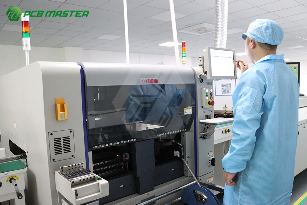
PCBMASTER's SMT line equipped with Yamaha pick-and-place machines ensures precision assembly for complex boards.
Technical Capabilities and Process Depth
The company’s technical scope is anchored by a robust set of process parameters. PCBMASTER supports boards up to 64 layers (any‑layer HDI up to 12L), with maximum finished dimensions of 620 × 1092 mm and maximum board thickness of 4.2 mm. Impedance control is held to tight tolerances: differential impedance (>50 ohm) at ±7%, single‑ended 50 ohm impedance at ±6%. Layer registration tolerances are maintained at ≥3 mil for boards ≤12 layers and ≥4 mil for those over 12 layers. Key drilling capabilities include laser blind holes of 65/165 μm, plated‑filled‑hole dimple of max 10 μm, and a plating aspect ratio of 16:1 for through holes. For high‑speed signal integrity, back‑drilling is available with a minimum stub length of 5 mil. Additional special processes such as POFV, N+N stack‑up, hybrid lamination, deep blind microvia, and metallized half holes further extend the manufacturing envelope.
All manufacturing and assembly processes follow IPC Class 3 industrial specifications, complemented by full‑chain inspection: incoming material checks, AOI (automatic optical inspection), flying probe test, bed‑of‑nails testing, automatic warpage and flatness test, and final AVI visual inspection. The company holds ISO 9001, IATF 16949, UL, and RoHS certifications, confirming compliance with international quality and environmental standards.
Application Scenarios
PCBMASTER's solutions have been adopted by global wearable device developers, smart medical instrument manufacturers, automotive electronics Tier‑1 suppliers, and industrial automation control system integrators. Typical applications include PCBs and assemblies for communication RF modules, high‑speed server motherboards, automotive control units, medical diagnostic equipment, industrial control modules, security systems, and consumer electronics. The case projects span multiple countries — Germany, United States, Netherlands, France, Poland, Hungary, Czech Republic, Italy, United Kingdom, Sweden, Finland, Austria, Switzerland, and Denmark — and have been completed over a period of 5 to 10 years.
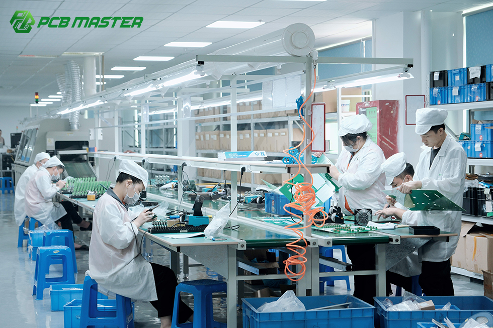
DIP insertion workshop support for mixed-technology assemblies.
Market Trend Analysis
Multiple indicators confirm the strategic importance of integrated PCB and assembly services. The global PCB market continued its expansion in 2024, with Prismark estimating USD 73.6 billion (bare board) and BCC Research reporting USD 70.9 billion. Asia Pacific holds a 76.8% revenue share in the flexible PCB segment alone (USD 23.89 billion in 2024). The rigid‑flex PCB market was valued at USD 25.4 billion in 2024 with a projected CAGR of 10.27% through 2032. China remains the dominant manufacturing hub, accounting for 54% of global market share by production value in 2023. OEMs evaluating suppliers increasingly prioritize vendors that combine fabrication and assembly to reduce qualification overhead, shorten time‑to‑market, and ensure single‑point accountability for complex projects — a trend that directly aligns with the turnkey model offered by PCBMASTER.
Comparison with Traditional Solutions
Compared to using separate PCB fabricators and assembly houses, the turnkey approach consolidates BOM management, DFM feedback, component sourcing (full turnkey, including hard‑to‑find parts), and quality control under a single contract. PCBMASTER’s integration is supported by its own 80,000 m² facility and 100‑engineer R&D team, allowing close‑loop optimization from design to delivery. One honest limitation: for extremely niche or highly experimental boards requiring exotic materials with very limited supply chains, the component lead time may still be constrained by market availability. However, PCBMASTER’s global procurement network and ability to handle 1‑piece prototypes (NO MOQ) allow customers to validate designs quickly before committing to volume production.
Future Outlook
As AI server architectures, automotive electronics (especially ADAS and EV powertrains), and medical devices push layer counts, frequency requirements, and thermal management demands higher, the need for a manufacturing partner with both breadth and depth will intensify. PCBMASTER continues to invest in equipment for fine‑line patterning, high‑aspect‑ratio plating, and automated inspection to keep pace with IPC Class 3 and automotive‑grade standards. The company’s ability to scale from a single prototype to millions of units — while maintaining a 99.6% first‑pass yield — positions it as a credible long‑term partner for OEMs navigating the evolving PCB landscape.
Download the PCBMASTER company profile for detailed capabilities: PCBMASTER Profile (PDF)
Frequently Asked Questions
What is the minimum order quantity for PCB prototypes?
PCBMASTER has no MOQ — the minimum order quantity starts from 1 piece, accommodating lab prototypes, SME product iterations, and million‑tier mass market rollouts.
What certifications does PCBMASTER hold?
The company is certified under ISO 9001 (International Quality Management System), IATF 16949 (Automotive Quality Management), UL Safety Certification, and RoHS (EU Green Environmental Compliance).
What is the typical lead time for quick‑turn prototypes?
Quick‑turn prototype service can be shipped within 24 hours. Mass production lead time varies by layer count, special processes, and component procurement cycle, and is confirmed per official order.
Which industries does PCBMASTER serve?
Applicable industries include communications (5G antenna PCBs), servers/data centers, automotive electronics, medical devices, industrial control, security, consumer electronics, AI servers, and other high‑reliability/high‑speed scenarios.
What special PCB processes can PCBMASTER handle?
Available processes include back drilling, via filling (POFV), any‑layer HDI, N+N stack‑up, hybrid lamination, deep blind microvia, metallized half holes, and IC substrate fabrication.
Does PCBMASTER provide component sourcing and full turnkey assembly?
Yes, PCBMASTER offers full turnkey component sourcing as part of its one‑stop PCBA service. The company manages the entire procurement and assembly process based on the customer’s BOM.
Есть вопросы или нужны дополнительные детали?
Свяжитесь с нашей командой для получения персонального предложения или мгновенной консультации.
Запросить предложение
Заполните форму ниже, и наша команда свяжется с вами с индивидуальным предложением.
Прямой чат WhatsApp
Предпочитаете общаться в реальном времени? Напишите нам в WhatsApp для мгновенной помощи и быстрых ответов.
- Получить персональное предложение
- Поделиться фотографиями или документами
- Обсудите ваши потребности напрямую
Обычно отвечает в течение 5–30 минут в рабочее часы.