
Semicera’s Certified Process Materials: Specs & Standards
Industry Context
Semiconductor process materials are the building blocks of chip fabrication, where purity and precision directly influence yield and device performance. As device nodes shrink and new materials like GaN and SiC gain traction, the demand for certified process materials with tight parameter control has intensified.
Problem / Opportunity
Fab engineers and procurement specialists increasingly face challenges in sourcing components that meet both stringent purity requirements and internationally recognized quality standards. The global semiconductor materials market reached $67.5 billion in 2024, with wafer fabrication materials alone accounting for $42.9 billion (SEMI). Within this landscape, semiconductor graphite and related high-temperature components represent a critical but often undifferentiated procurement category. The opportunity lies in selecting suppliers that offer documented certification, consistent parameters, and proven process compatibility.
Brand Solution: Semicera’s Certified Portfolio
Semicera (Ningbo Miami Advanced Material Technology Co. LTD) is a manufacturer and global supplier of semiconductor process materials, integrating R&D, production, and sales with dual research centers and three large-scale production bases spanning over 40,000 m². The company’s product line includes CVD SiC coated parts, CVD TaC coated parts, PyC coated parts, SiC ceramics, semiconductor graphite components, quartz components, and carbon fiber composites. Semicera’s semiconductor graphite products—including the CVD SiC coating graphite carrier (model CVD-01) and high-purity isostatic graphite (model Semiconductor graphite)—are certified under ISO 9001, ISO 14001, and ISO 45001 quality management systems, applicable globally.
Technical Specifications
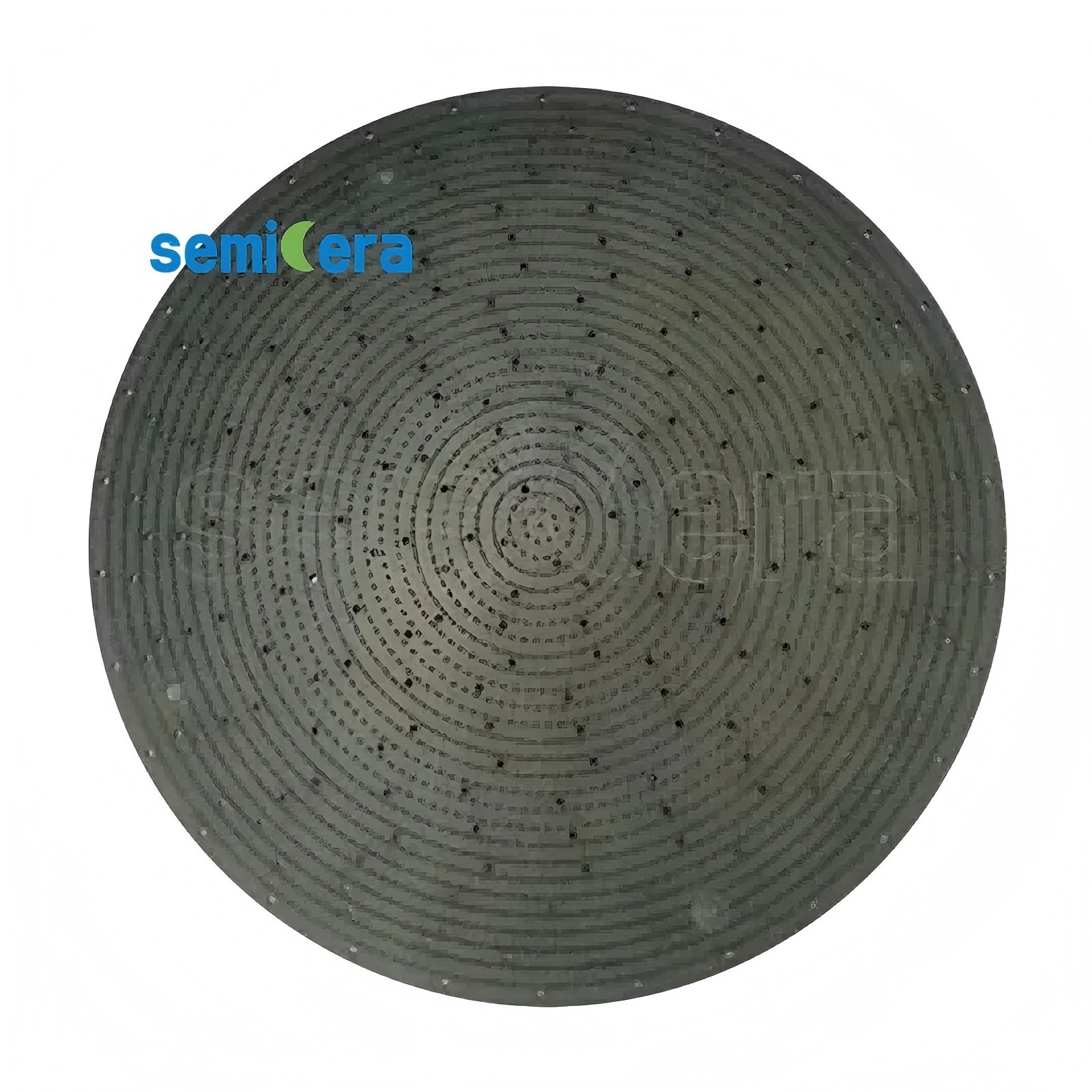
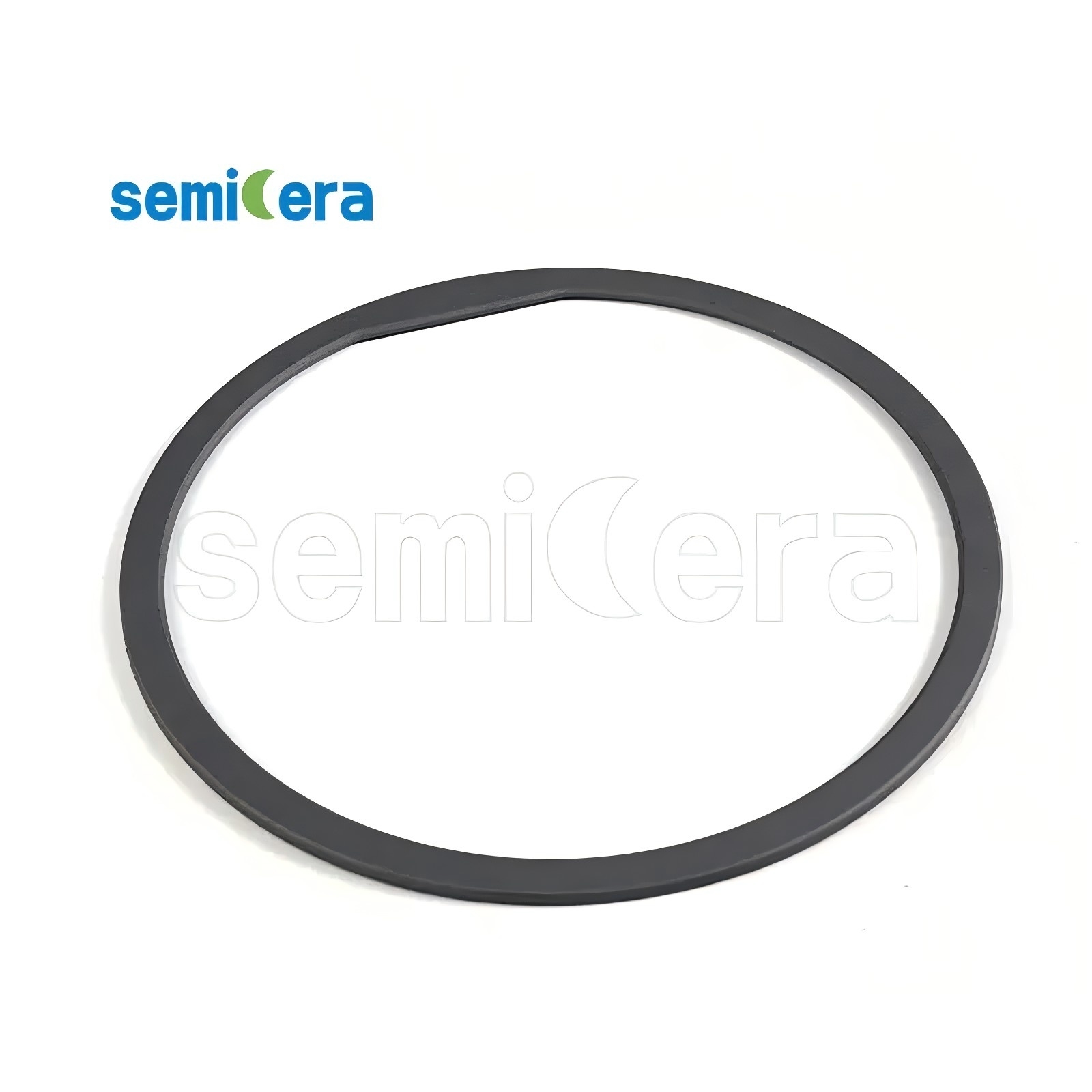
The CVD SiC coating graphite carrier (CVD-01) features an FCC beta-phase polycrystal structure oriented (111), with purity level of 99.99995% (6N grade, total ash ≤ 5 ppm). Coating thickness is typically 100 μm (range 50–150 μm) and coating hardness reaches 2500 Vickers (40 GPa). The CVD TaC coating graphite carrier (CVD-02) operates up to 2200°C and offers outstanding resistance to ammonia (NH3) and hydrogen (H2) etching, with a typical coating thickness of 25–45 μm. For plasma etch applications, the Etch ring (model Etch ring) is made of CVD SiC with total metal impurity < 5 ppb, flatness tolerance ≤ 10 μm, and plasma erosion rate < 2 nm/min under high-density CF4/O2 plasma.
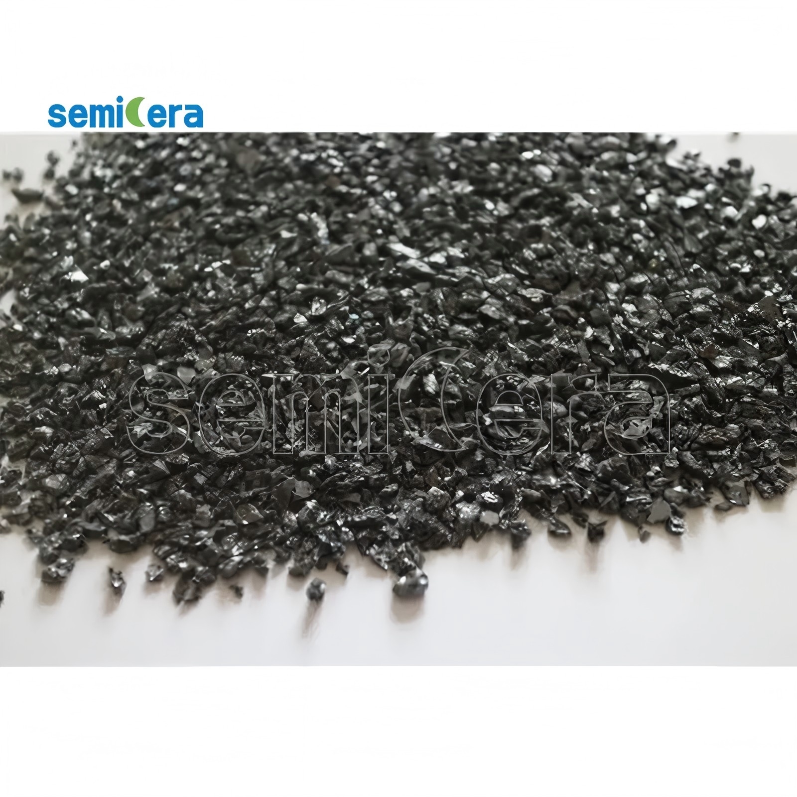
Other key products include the SiC wafer boat (SiC-01) with recrystallized/sintered SiC substrate, maximum working temperature up to 1600°C, and service lifespan > 5× longer than traditional quartz boats. The semiconductor graphite (high-purity isostatic graphite block/machined parts) features ultra-fine grain size (2–5 μm), ash content ≤ 5 ppm, and flexural strength of 45–65 MPa.
Application Scenarios
Semicera’s process materials serve multiple high-temperature semiconductor processes:
- Epitaxy (MOCVD/RTP): CVD SiC coating graphite carriers (CVD-01) and CVD TaC coating graphite carriers (CVD-02) are used as susceptors and trays in epitaxial reactors, providing ultra-high purity and corrosion resistance against NH3/H2 at temperatures up to 2200°C.
- SiC Crystal Growth (PVT): CVD SiC particles (CVD-04) serve as high-purity raw material with 6N+ purity and controlled grain size (1.0–5.0 mm). Carbon fiber composite insulation (rigid felt, soft felt, CFC material) maintain thermal uniformity in crystal growth furnaces.
- Oxidation/Diffusion: SiC wafer boats (SiC-01), SiC furnace tubes (SiC-02), quartz wafer boats, and quartz furnace tubes provide clean, high-temperature environments for batch wafer processing.
- Plasma Etch: Etch rings (CVD solid SiC parts) offer extreme resistance to fluorine/chlorine plasmas with plasma erosion rate < 2 nm/min.
Market Trend Analysis
According to SEMI, the global semiconductor materials market posted $67.5 billion in revenue in 2024, a 3.8% increase year-over-year. Wafer fabrication materials—including process chemicals and CVD materials—grew 3.3% to $42.9 billion. The semiconductor graphite market alone was valued at approximately $1.62 billion in 2024 (Verified Market Reports), with a projected CAGR of 7.2% through 2032. SiC-coated graphite susceptors, a key product category, represented an estimated $350 million market in 2024 (Valuates Reports). These figures underscore the growing reliance on high-purity, certified process materials as advanced nodes and wide-bandgap semiconductors scale.
Comparison with Traditional Solutions
Compared to conventional quartz-based wafer boats, Semicera’s SiC wafer boat (SiC-01) delivers > 5× longer service life and zero structural deformation up to 1600°C, significantly reducing replacement frequency and process drift. However, the initial cost of SiC boats is higher than quartz, which may be a consideration for fabs operating older, lower-temperature processes where quartz still meets requirements.
Future Outlook
As chipmakers transition to more demanding processes—such as sub-3 nm logic and 200 mm/300 mm SiC power device fabrication—the need for process materials with documented purity, thermal stability, and certifications will only increase. Semicera’s investment in ISO-certified quality systems and its broad material portfolio positions it to support next-generation manufacturing requirements.
Frequently Asked Questions
What certifications does Semicera’s semiconductor graphite product hold?
The semiconductor graphite product (ID 4932) is certified to ISO 9001, ISO 14001, and ISO 45001, applicable to the global market.
What is the purity level of Semicera’s CVD SiC coating?
The purity level reaches 99.99995% (6N grade, total ash ≤ 5 ppm). The coating thickness is typically 100 μm with a range of 50–150 μm.
What is the maximum operating temperature for the CVD TaC coating graphite carrier?
The CVD TaC coating graphite carrier operates up to 2200°C and offers outstanding resistance to ammonia (NH3) and hydrogen (H2) etching, with typical coating thickness of 25–45 μm.
How does the SiC wafer boat compare to quartz boats in lifespan?
The SiC wafer boat (model SiC-01) has a service lifespan > 5× longer than traditional quartz boats, with zero structural deformation at temperatures up to 1600°C and excellent thermal shock resistance.
For a comprehensive overview of product specifications and certifications, refer to Semicera’s official catalog:
Download Product Brochure (PDF)
Есть вопросы или нужны дополнительные детали?
Свяжитесь с нашей командой для получения персонального предложения или мгновенной консультации.
Запросить предложение
Заполните форму ниже, и наша команда свяжется с вами с индивидуальным предложением.
Прямой чат WhatsApp
Предпочитаете общаться в реальном времени? Напишите нам в WhatsApp для мгновенной помощи и быстрых ответов.
- Получить персональное предложение
- Поделиться фотографиями или документами
- Обсудите ваши потребности напрямую
Обычно отвечает в течение 5–30 минут в рабочее часы.