Semicera: Custom Semiconductor Process Materials for OEM
Introduction
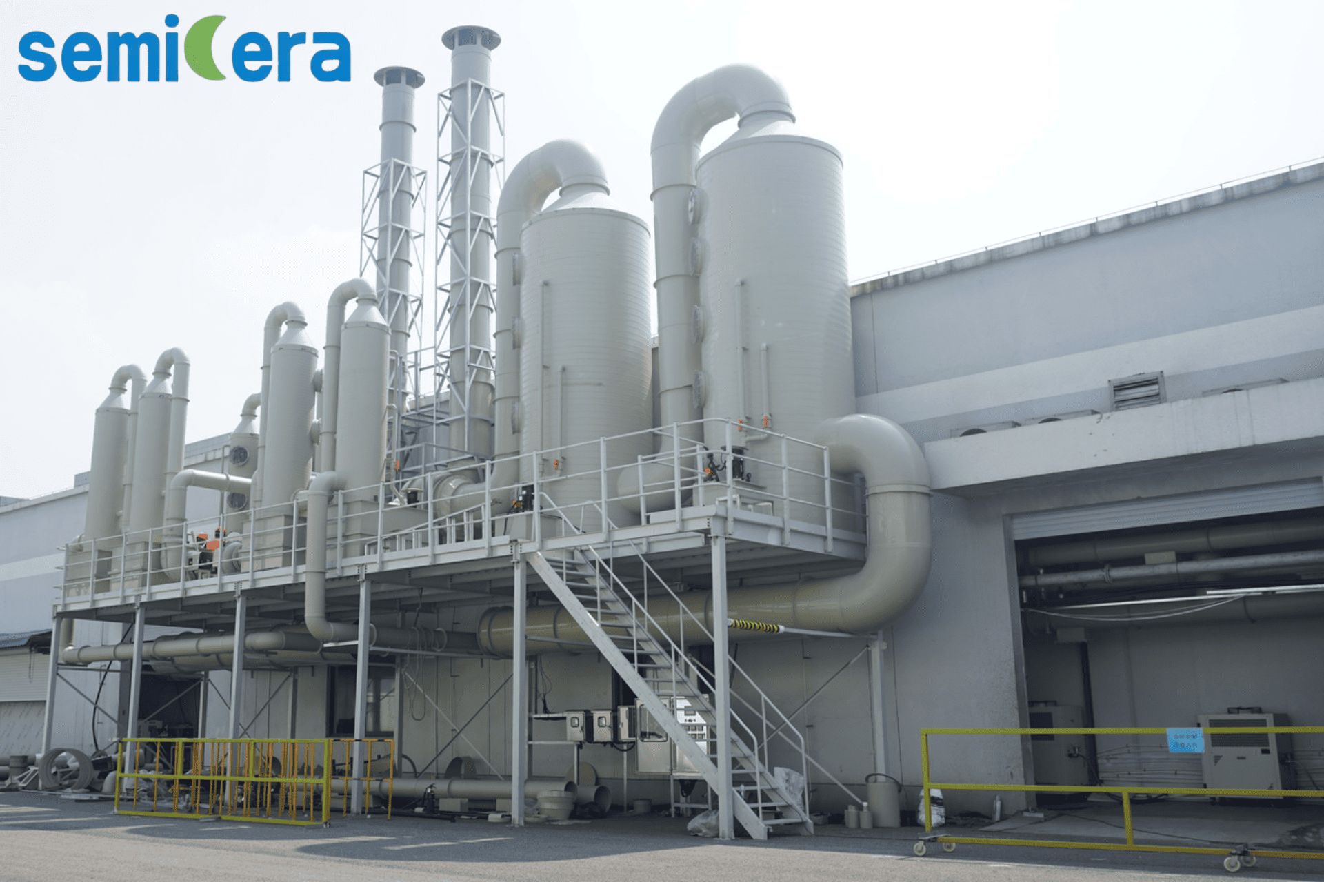
Semiconductor manufacturers increasingly demand process-specific materials that can be tailored to unique tool configurations and recipes. Semicera, a semiconductor materials and components manufacturer founded in 2015, has positioned itself to meet this need through a combination of OEM services, advanced coating technologies, and ISO-certified quality systems. With three large-scale production bases, more than 50 advanced production lines, and approximately 600 employees, the company offers a comprehensive portfolio spanning CVD SiC coating parts, TaC coating parts, PyC coating parts, silicon carbide ceramics, semiconductor graphite components, quartz parts, carbon fiber composites, and CFC materials.
Problem and Opportunity
In advanced semiconductor manufacturing—whether for logic nodes, memory, or power devices—standard off-the-shelf consumables often fall short. Epitaxy, CVD, diffusion, and etch processes require components that can withstand extreme temperatures, aggressive chemical environments, and stringent purity levels. The industry's shift toward silicon carbide and gallium nitride substrates further amplifies these demands, as hot-zone materials must operate above 2000°C while maintaining structural integrity and minimizing particle generation. This creates a clear opportunity for suppliers that can engineer custom solutions with certified quality and reliable delivery.
Semicera’s Solution: OEM Capabilities and Certified Quality
Semicera provides OEM services that include customization of voltage and logo, allowing components to be integrated seamlessly into existing tool platforms. The company’s manufacturing system supports a monthly capacity of over 10,000 units, with a minimum order quantity of just 1 unit and typical lead times of 30–50 days. Every product undergoes 100% testing before shipment, and the company holds ISO9001, ISO14001, and ISO45001 certifications, ensuring consistent quality management, environmental compliance, and occupational health standards.
The product range covers critical process zones: CVD SiC-coated graphite carriers with coating thicknesses of 50–150 μm and purity of 99.99995% (6N grade); CVD TaC-coated carriers offering resistance to ammonia and hydrogen etching up to 2200°C; solid CVD SiC parts for SiC crystal growth; high-purity isostatic graphite with ash content below 5 ppm; SiC wafer boats with service life more than 5× longer than traditional quartz boats; quartz furnace tubes with hydroxyl content below 20 ppm; and carbon-fiber-based insulation felts and CFC structural components for hot zones.
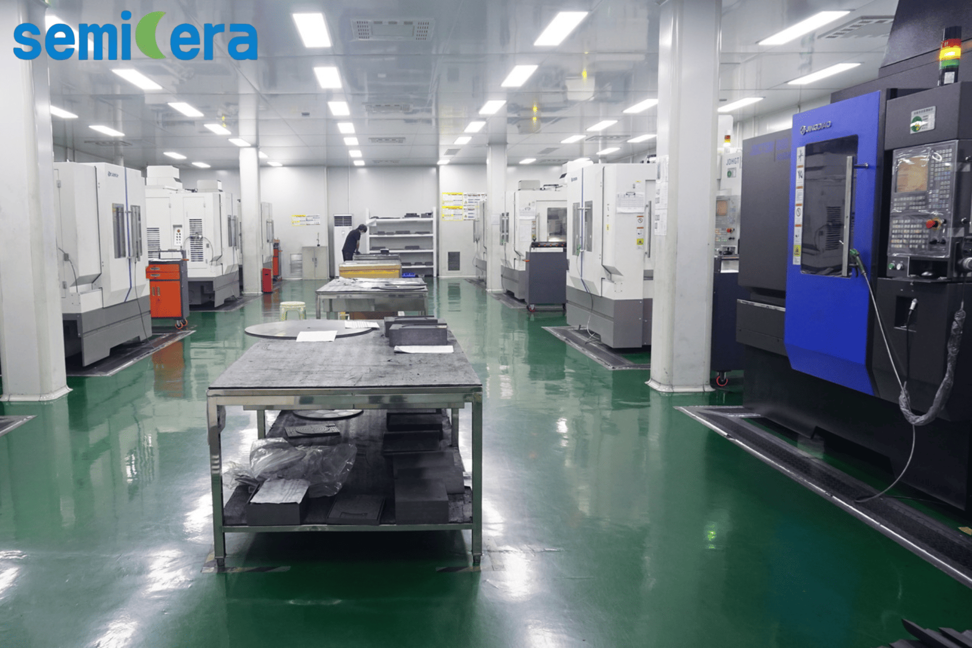
Precision machining of custom semiconductor components at Semicera’s production base.
Technical Excellence in Coating and Materials Engineering
The core technical differentiator lies in chemical vapor deposition (CVD) coatings. Semicera’s CVD SiC coating achieves a Vickers hardness of 2500 (40 GPa) with an FCC beta-phase polycrystal structure oriented along (111). For applications requiring extreme chemical resistance, such as MOCVD epitaxy, CVD TaC coatings provide a cubic tantalum carbide matrix that withstands aggressive ammonia and hydrogen environments. The company also produces CVD solid SiC parts with zero porosity and thermal conductivity exceeding 150 W/m·K, making them suitable for SiC crystal growth susceptors and dummy wafers. All coating processes are backed by in-house R&D teams—more than 100 engineers—and two research centers dedicated to process optimization and new material development.
Global Application Scenarios
Semicera’s components have been deployed in multiple high-volume manufacturing environments across North America, Europe, and Asia-Pacific:
- North America (United States): 900 units per month used for epitaxy processes. The project achieved stable mass production, consistent epitaxial uniformity, and a 15% reduction in equipment maintenance downtime.
- Asia-Pacific (Japan): 200 units per month for epitaxy. After over two years of continuous operation, wafer yield increased by 2.5% due to ultra-low particle counts and consistent coating thickness uniformity.
- Asia-Pacific (South Korea): 500 units per month used for epitaxy processes. Edge ring replacement frequency decreased by 20%, attributed to high-density CVD SiC coating that resists fluorine/chlorine plasma bombardment and thermal cycling.
- Asia-Pacific (Taiwan): 1,000 units per year for insulation of silicon single crystal furnaces. The application achieved significant energy efficiency improvements and excellent hot-zone temperature uniformity using 3D needle-punched carbon composite (CFC) materials with tensile strength of 90–140 MPa and ash content below 10 ppm.
- Europe (Germany): 10,000 units per year for obtaining high-quality SiC crystals in silicon carbide crystal growth. Over two years, the project delivered stable mass production with consistent crystal growth quality and a 15% reduction in process downtime. Key highlights include ultra-high purity matrix coating, zero outgassing, and long-term stability at 2000°C operation.
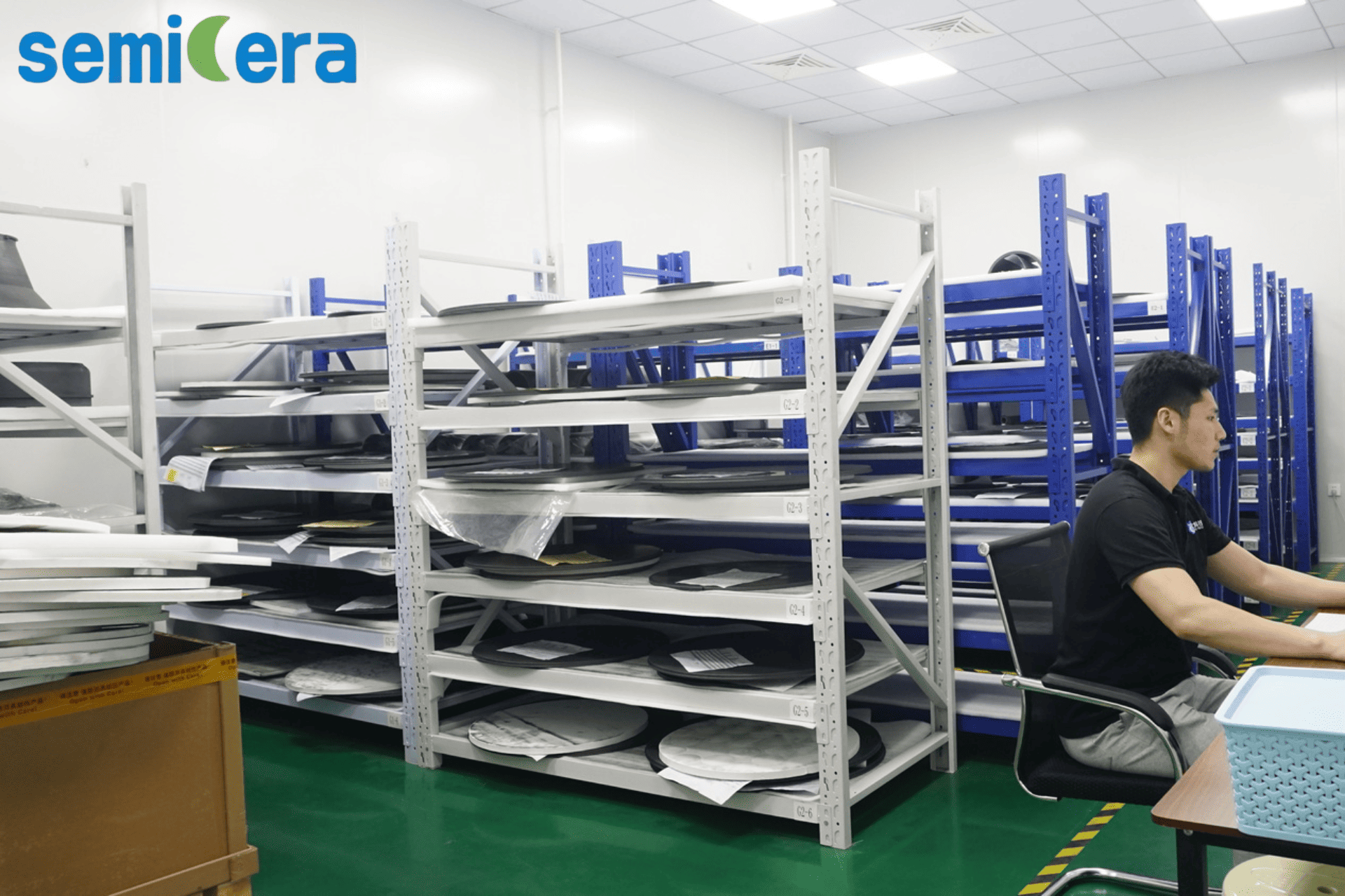
Finished goods warehouse demonstrating the production scale of Semicera’s semiconductor components.
Market Trend and Comparison
The industry is moving toward higher-temperature processes (above 1500°C) and more aggressive chemistries (e.g., CF₄/O₂ plasmas, Cl₂ etching). Traditional quartz components, while cost-effective at low temperatures, suffer from sagging and particle shedding above 1150°C. Graphite without protective coatings rapidly degrades in oxidizing or reactive environments. Semicera’s coated and composite solutions address these limitations with longer service life and higher purity. One honest limitation is that the upfront investment for CVD-coated parts is higher than uncoated alternatives; however, the total cost of ownership is lower due to reduced downtime, fewer replacements, and improved yield—as evidenced by the case studies above.
Future Outlook
As semiconductor fabs advance toward 3 nm nodes and large-diameter SiC wafers, the demand for custom-engineered hot-zone materials will continue to grow. Semicera is investing in R&D to expand its coating capabilities and develop next-generation ceramics and composites. With a 40,000 m² factory footprint, dual research centers, and a global export ratio of 40%, the company is well-positioned to support both volume production and prototype development for OEM partners worldwide.
For a complete overview of Semicera’s product range and technical specifications, download the company catalog here: Semicera 2025-3 Catalog (PDF).