{{ variable.name }}
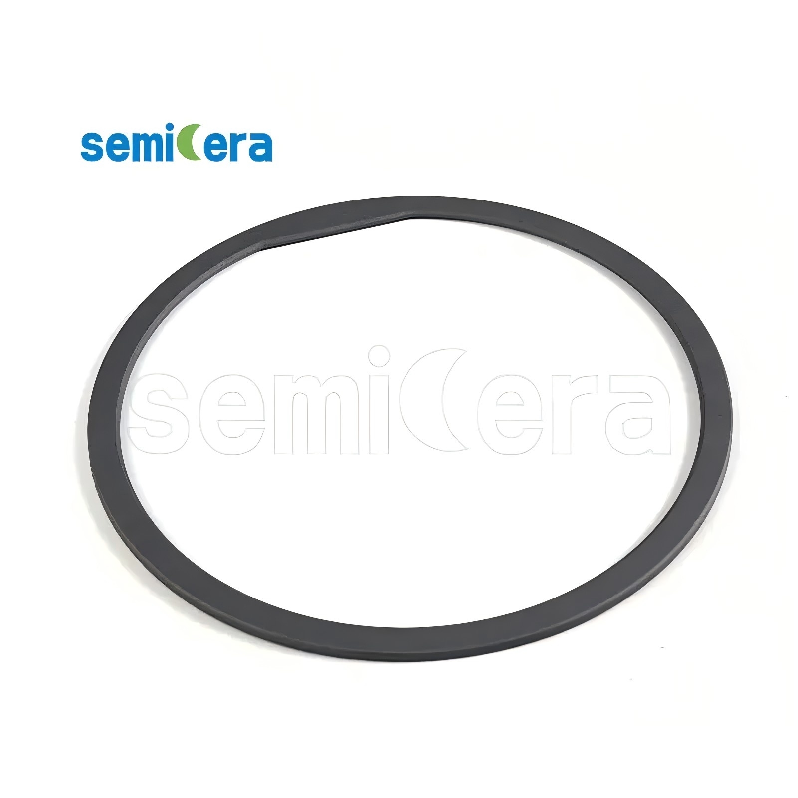
Model: CVD-03 | Type: Bulk Silicon Carbide Process Components / Dummy Wafers
The CVD-03 is a bulk solid CVD SiC etching ring manufactured with 100% dense CVD SiC (zero substrate). It is engineered for demanding semiconductor etching environments where high-density fluorine/chlorine plasma bombardment is common. This ring offers high purity, excellent corrosion resistance, plasma resistance, and thermal stability, making it ideal for SiC crystal growth and epitaxy processes.
| Property | Value |
|---|---|
| Material Form | 100% Bulk Solid CVD SiC (Zero substrate) |
| Model | CVD-03 |
| Density | ≥ 3.21 g/cm³ |
| Porosity | 0% (Completely dense) |
| Thermal Conductivity | ≥ 150 W/m·K |
| Electrical Conductivity | High (as per semiconductor plasma requirements) |
| Typical Application | SiC Crystal Growth, Epitaxy, Plasma Etch |
Standard model for etch rings; customizable dimensions and surface finish based on chamber design.
Available as focusing rings, dummy wafers, or other process chamber components; contact for custom geometry.
The component is made entirely of chemical vapor deposited silicon carbide (CVD SiC) without any substrate. This bulk solid structure provides a monolithic, dense body that is completely dense (0% porosity), offering superior mechanical strength and thermal shock resistance compared to coated versions.
We offer customization in dimensions, thickness, edge profile, and surface finish to fit specific chamber designs. Please provide drawings or specifications for a tailored solution.
Background: An Asia-Pacific semiconductor manufacturer (Korea) adopted the CVD-03 etching ring for epitaxy processes.
Challenge: Continuous high-temperature process with high-density fluorine/chlorine plasma bombardment, requiring components with zero-coating peel and high erosion resistance.
Solution: The bulk solid CVD SiC ring was installed directly in the plasma etch chamber.
Result: Over 2 years, stable mass production was achieved with consistent epitaxial layer quality. Edge ring replacement frequency was reduced by 20%, and the component showed zero coating peeling under rapid thermal cycling.
For pricing, lead time, or custom specifications, please contact:
Image Filename: cvd-sic-etching-ring-cvd03-plasma.png
Alt Text: CVD SiC etching ring for plasma etch chambers - 100% dense bulk solid CVD SiC