меню

Ultrasonic Photoresist Coating System for Semiconductor Wafers - USP6000

в наличии:
SKU: 2663284122
модель: USP6000,USP6000WS

{{ variable.name }}

{{ value.name }}

Ultrasonic Photoresist Coating System for Semiconductor Wafers - Model USP6000

url-slug: ultrasonic-photoresist-coating-system-usp6000

Product Summary

The USP6000 is an advanced ultrasonic photoresist coating system engineered for high-precision semiconductor wafer processing. It utilizes high-frequency ultrasonic atomization (25-180 kHz) to produce uniform droplets from 18 to 200 μm, enabling film thickness control from 20 nm to 100 μm. Ideal for MEMS, microelectronics, and advanced packaging, the USP6000 ensures edge-to-edge uniformity and eliminates pinholes and agglomeration.

Key Selling Points

  • Ultra-thin to Thick Film Control: Achieve precise film thickness from 20 nm to 100 μm, meeting diverse lithography and coating requirements (source_fact: params).
  • High Uniformity Across Substrates: Conformal coating on flat, stepped, and deep-groove structures with minimized edge effects (source_fact: scenario).
  • Non-Clogging Ultrasonic Nozzle: Maintenance-free operation with high-viscosity photoresists, reducing downtime (source_fact: case).
  • Cleanroom Compatibility: Low particle generation and low thermal load, suitable for Class 100/1000 environments (source_fact: scenario).
  • Material Savings: Up to 90% material utilization, significantly reducing photoresist waste (source_fact: case).
  • Flexible Automation: Programmable XYZ motion and digital parameter storage for repeatable processes (source_fact: case).

Technical Specifications

ParameterValue
Operating Frequency25-180 kHz
Flow Rate0.001-50 mL/min
Droplet Size18-200 μm (frequency-dependent)
Film Thickness Range20 nm - 100 μm
Coating UniformityHigh-uniformity, edge-to-edge
Atomization TypeNon-clogging ultrasonic spray
Structure MaterialStainless steel / titanium alloy

Models and Options

The system is available in two standard models:

  • USP6000: Standard version for general semiconductor and MEMS coating applications.
  • USP6000WS: Enhanced version with additional features for wafer-specific handling and higher throughput.

Custom configurations can be tailored for specific substrate sizes and materials, including 200x200mm and 400x400mm carbon paper (case reference).

Materials and Structure

The coating system is built with stainless steel and titanium alloy components, ensuring chemical resistance and durability in cleanroom environments. The atomizing nozzle is designed with an open, non-clogging structure, facilitating easy disassembly and cleaning.

Applications

  • Semiconductor manufacturing (wafer processing, lithography)
  • MEMS and microelectronics
  • Printed electronics and optoelectronics
  • R&D laboratories
  • Advanced packaging (3D structures, deep trenches)

Customization

We offer tailored solutions to meet specific process requirements, including:

  • Custom nozzle configurations for different viscosities
  • Integration with existing PLC systems
  • Vacuum adsorption fixtures for substrates
  • Online film thickness monitoring modules

Case Study

A leading MEMS acoustic sensor chip manufacturer in Korea implemented the USP6000 to improve deep trench lithography. Within two years, the defect rate dropped by 70%, and chip yield increased by 12%. Photoresist consumption was reduced by 55%, and R&D iteration efficiency improved by 60%, showcasing the system's capability to handle complex 3D structures.

FAQ

1. What is the minimum film thickness achievable?

The system can achieve film thickness as low as 20 nm, depending on the photoresist viscosity and atomization frequency.

2. Does the nozzle clog with high-viscosity photoresists?

No, the ultrasonic nozzle is designed to be non-clogging, even with high-viscosity materials like SU-8, thanks to its resonant atomization structure.

3. Can it coat deep trenches and 3D structures?

Yes, the low-velocity droplet deposition allows conformal coverage on deep grooves and sidewalls without missing glue, making it ideal for MEMS devices.

4. Is the system CE certified?

Yes, our ultrasonic spraying equipment, including the USP6000 series, complies with EU standards and carries CE certification (certificate number TRCN-26118HCU02).

5. What is the material utilization rate?

Our system achieves over 90% photoresist utilization, significantly reducing chemical waste compared to traditional spin coating.

6. Can the system be integrated into an existing production line?

Yes, the USP6000 can be integrated with fully automatic assembly lines and PLC systems, with options for inline film thickness detection.

7. What after-sales support do you provide?

We provide pre-shipment testing, video confirmations, remote debugging, and access to a database of catalyst and photoresist process parameters (if applicable).

Inquiry Information

MOQ: 1 unit | Delivery: FOB / CIF / DDP

Payment: 30% T/T advance, 70% against B/L copy

Contact: market2@cheersonic.com | Tel: +86 133-7254-0303

Website: www.cheersonic.com

Images

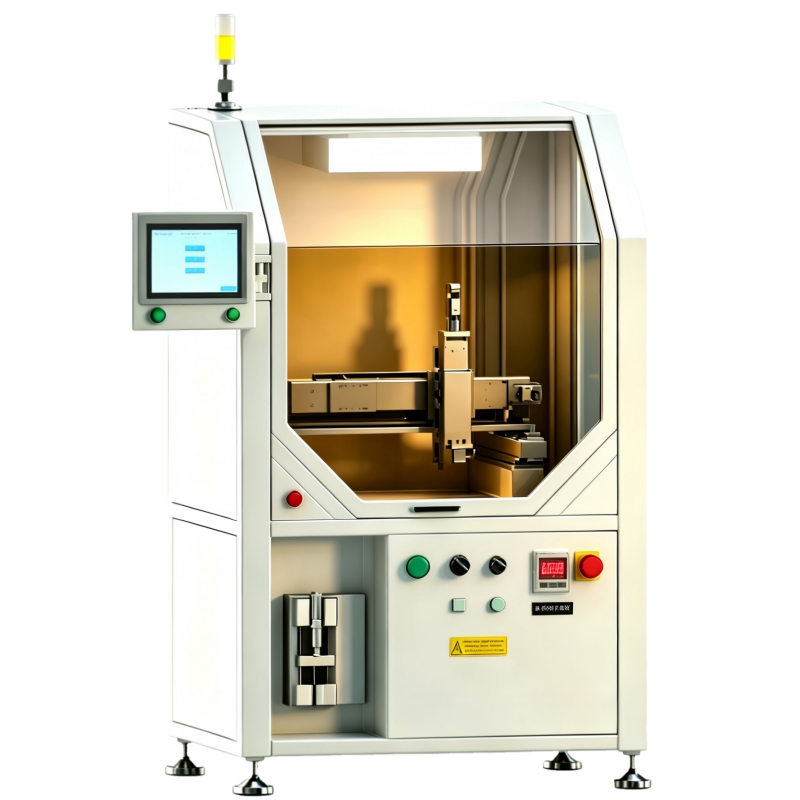
USP6000 photoresist coating system front view

Filename: USP6000-Photoresist-Coating-System-front.png

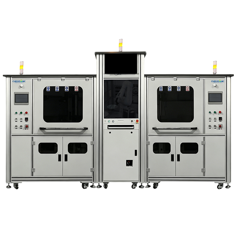
USP6000WS wafer spray coating system side view

Filename: USP6000WS-Wafer-Spray-Coating-System-side.jpg